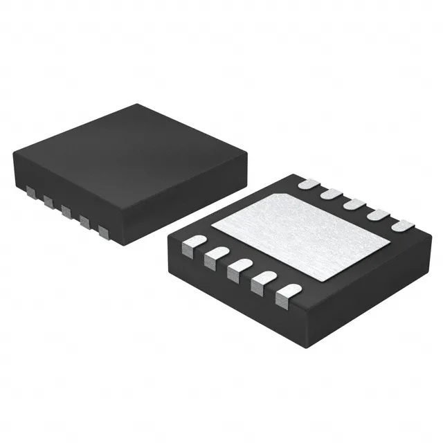
10-TDFN exposed-pad footprint and board integration
The MAX4636ETB+T: The datasheet's recommended footprint calls for a single central pad matching the paddle size, with via stitching to an inner ground plane if the switch carries continuous current near the 4 Ohm on-resistance limit. No MSL floor-life concern beyond the standard Level 1 bake-out for exposed-pad packages.
4 Ohm on-resistance and channel matching for precision signal routing
For a 10 kOhm load, the 4 Ohm adds 0.04 % insertion loss; for a 50 Ohm RF path it drops 0.5 dB, so the part suits low-frequency analog multiplexing better than RF switching. Channel-to-channel matching is 100 mOhm max — the two SPDT halves track within 2.5 % of each other. This matters when the switch is used in a differential signal pair or a stereo audio path where gain mismatch between channels creates crosstalk or phase error. Each SPDT section implements a 2:1 multiplexer/demultiplexer — two inputs selectable to one common output, or one input routed to either of two outputs. The dual-circuit configuration gives two independent SPDT switches in the same package, sharing only the supply and ground pins.
Charge injection, leakage, and crosstalk — the signal-integrity budget
Charge injection is 2 pC typical — when the switch toggles, that amount of charge is dumped onto the load. Into a 10 pF sampling capacitor it creates a 200 mV glitch; into a 100 pF cap it drops to 20 mV. For precision ADC front-ends, the sampling capacitor must settle before the conversion starts, or the injected charge corrupts the reading. Off-leakage current is 100 pA max at 25°C — this is the current that leaks through the open switch into the signal path. In a high-impedance sensor circuit (10 MOhm source), 100 pA creates a 1 mV offset error; in a 1 kOhm circuit it is negligible at 0.1 µV. The leakage doubles roughly every 10°C, so at 85°C it approaches 1.6 nA — still manageable for most precision analog designs. Crosstalk is -67 dB at 1 MHz — this is the signal coupling from one channel to another when both are active. For a 1 Vpp signal on channel A, the feedthrough onto channel B is about 0.45 mVpp at 1 MHz. Below 100 kHz the crosstalk improves further; above 10 MHz it degrades as parasitic capacitance dominates.
Switching speed and supply flexibility
Turn-on time is 14 ns max, turn-off is 6 ns max — the switch transitions fast enough for 20 MHz clock multiplexing or video switching at standard-definition rates. The asymmetry (on slower than off) means the break-before-make timing is inherent: the off path opens 8 ns before the on path closes, preventing momentary short-circuits between inputs. The on-resistance rises at lower supply voltages — at 1.8 V the 4 Ohm max spec applies; at 3.3 V it typically drops to 2.5 Ohm. No dual-supply rail needed, which simplifies the power tree in mixed-voltage designs.
ROHS3 compliant — the part meets the latest EU restriction on hazardous substances, covering all ten restricted substances including the four phthalates added in 2015. No stock-holding claim; the part is procured per RFQ with full lot traceability and manufacturer warranty from authorized channels.