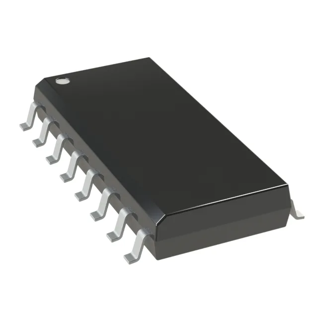
Analog Devices MAX4619CUE+ — Discrete Semiconductors

MAX4619CUE+ Analog Devices SPDT Switch, 10 Ohm, 16-TSSOP

MPNMAX4619CUE+
End of Life

Analog Devices MAX4619CUE+ CMOS analog switch, 3-circuit SPDT, 10 Ohm on-resistance, 15ns/10ns switching, -96dB crosstalk, 16-TSSOP, Tube.

$4.1Ref. price · indicative, final on quote
Packaging16-TSSOP (0.173", 4.40mm Width)
StockContact for availability
Lead timeIn Stock wk
MOQ1 pcs
  • 100% new & originalTraceable channels only — no refurbs, no pulls, no remarked parts.
  • Date & lot codes on quoteStated per line before you commit; label photos on request.
  • MSL-compliant ESD packingMoisture-sealed bags with indicator cards; reels photo-verified.
  • PayPal buyer protectionPay by T/T, PayPal or Payoneer — card payments covered end to end.

Specifications

MAX4619CUE+ Technical Specifications
ParameterValue
Mounting typeSurface Mount
Voltage - supply, single (V+)2V ~ 5.5V
Current - leakage (IS(off))1nA
Operating temperature0°C ~ 70°C (TA)
PackageTube
Crosstalk-96dB @ 100kHz
Case16-TSSOP (0.173\", 4.40mm Width)
Switch circuitSPDT
Charge injection3pC
Number of circuits3
On-State resistance10Ohm
Switch time (Ton, toff)15ns, 10ns
Multiplexer (Demultiplexer circuit)2:1
Channel capacitance (CS(off), CD(off))5pF, 8.5pF
Channel-to-Channel matching (ΔRon)200mOhm

Product details

10 Ohm on-resistance with 200 mOhm channel matching

The MAX4619CUE+ integrates three independent SPDT (single-pole double-throw) switch channels, each with a maximum on-resistance of 10 Ohm. The 200 mOhm channel-to-channel matching (ΔRon) keeps the resistance consistent across all three switches, which matters when the signal path gain or attenuation must track between channels in a multiplexed analog chain.

Switching speed and signal integrity for precision routing

Maximum turn-on time is 15 ns and turn-off time is 10 ns, so the switch can route audio or low-speed data paths at several megahertz without introducing timing skew between channels. The -96 dB crosstalk at 100 kHz means a signal on one channel couples into an adjacent channel at less than -96 dB below the signal level — adequate isolation for multiplexing multiple analog sensor inputs into a single ADC without bleed-through. Charge injection is 3 pC typical, which translates to a voltage glitch on the output when the switch transitions. For a 10 kOhm source impedance feeding a 10 pF sampling capacitor, that 3 pC injection creates roughly a 300 µV step — a number to budget in the acquisition time of a successive-approximation ADC. Off-leakage current is 1 nA maximum, and the channel capacitance measures 5 pF (source off) and 8.5 pF (drain off). Together these set the bandwidth of the off-channel isolation: the 8.5 pF drain capacitance forms a capacitive divider with the load, limiting isolation at high frequencies beyond what the -96 dB crosstalk spec covers.

Frequently asked questions

What is the on-resistance and does it change with temperature?

Maximum on-resistance is 10 Ohm at 25 °C. The datasheet's typical curve shows Rds(on) increasing by roughly 0.3 % per °C above 25 °C, so at 70 °C ambient the on-resistance is approximately 11.3 Ohm. The 200 mOhm channel-to-channel matching holds across the temperature range.

What does the -96 dB crosstalk spec mean in practice?

At 100 kHz, a 1 V signal on one channel couples into an adjacent off-channel at roughly 1.6 µV. This isolation is sufficient for multiplexing multiple 16-bit ADC inputs (78 dB SNR) without the crosstalk degrading the noise floor.