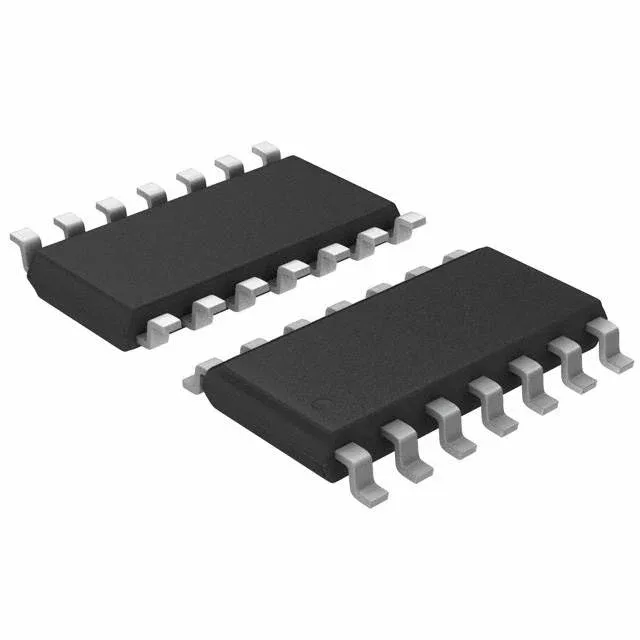
Quad SPST-NO switch with 10 Ohm Ron and 70 MHz bandwidth
The MAX4614ESD+T: The 10 Ohm max on-resistance sets the signal attenuation floor — for a 50 Ohm system, the insertion loss is about 0.8 dB, which is manageable for most analog paths but worth budgeting in a precision chain. The -3 dB bandwidth of 70 MHz means the switch passes composite video and baseband signals up to that frequency with less than 3 dB roll-off. For a 10 MHz analog signal, the flatness is well within 0.1 dB, making this part suitable for video routing or high-speed data acquisition front-ends. Crosstalk is rated at -96 dB at 100 kHz — that is the isolation between adjacent channels when one is active and the other is off. In a multiplexed ADC input stage, this level of separation keeps the channel-to-channel bleed well below the noise floor of a 16-bit converter at moderate sampling rates.
Switching speed and charge injection — timing and glitch budget
Turn-on and turn-off times are 12 ns and 10 ns max respectively. For a multiplexed bus cycling between four channels at 10 MHz, the switching transient occupies about 12% of the period — the downstream sample-and-hold must settle after the break-before-make interval. The 6.5 pC charge injection is the amount of charge dumped onto the load when the switch toggles; in a 10 pF sampling capacitor, that translates to a 650 mV glitch, so the hold capacitor needs to be large enough to absorb it or the sample window must be delayed past the glitch. Channel-to-channel on-resistance matching is 200 mOhm max. In a gain-set resistor network or a precision attenuator, this mismatch contributes a gain error of about 0.2% across channels — acceptable for 8-bit systems but worth a calibration step for 12-bit or higher.
Supply range and leakage — single-rail operation and high-impedance nodes
Operates from a single supply between 2 V and 5.5 V. At 3.3 V the switch is fully specified; at 2 V the on-resistance rises but remains within the 10 Ohm max spec. The 1 nA max off-leakage current means the switch does not load high-impedance nodes — a 10 MOhm source sees less than 10 mV of offset from leakage, negligible for most sensor interfaces. Channel capacitance is 5 pF for both source and drain when off. This capacitance combines with the source impedance to form a low-pass filter — with a 10 kOhm source, the -3 dB corner is about 3.2 MHz, so the bandwidth of the signal path is limited by the source impedance, not the switch itself.
Package and temperature grade — board-fit and deployment envelope
Housed in a 14-SOIC package (0.154-inch body width, 3.90 mm) with a surface-mount footprint. The supplier device package is also 14-SOIC, so no footprint ambiguity. The 1.27 mm pin pitch is standard — no fine-pitch routing challenges, and the package is compatible with most automated optical inspection systems. This is the industrial temperature band — suitable for factory-floor equipment, outdoor telecom enclosures, and automotive cabin environments, but not for under-hood or engine-bay deployment where 125°C ambient is common. Available in Tape & Reel (TR) or Cut Tape (CT) — the TR format is feeder-ready for high-volume pick-and-place lines; CT suits prototype or low-volume builds without minimum reel commitment.
RoHS3 compliant (2011/65/EU + 2015/863), so it ships without the six restricted substances plus the four phthalates.