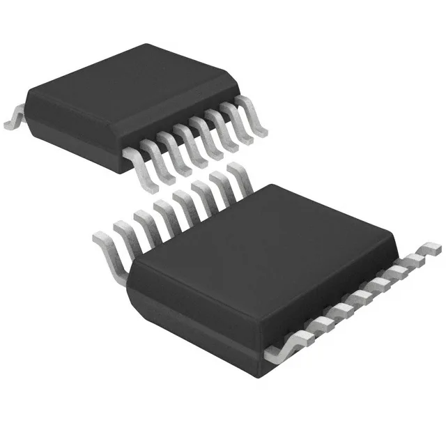
The MAX4602CAE+T is a quad SPST-NO analog switch from Analog Devices with a maximum on-resistance of 2.5 Ohm. For a precision analog signal path, this low Ron means the voltage drop across the switch stays under 2.5 mV per mA of signal current — negligible in a 10 V full-scale system but worth budgeting in a 0-5 V or 0-2.5 V single-supply front-end. Channel-to-channel matching is specified at 100 mOhm max, so the gain error introduced by the switch resistance is consistent across all four channels. This matters when the switch is used in a multi-channel data acquisition system where each channel must see the same source impedance.
Supply voltage range and power rail flexibility
The single-supply range covers common industrial rails (5 V, 12 V, 24 V) without needing a negative rail. The dual-supply option allows the switch to pass bipolar signals symmetrically around ground — useful for audio or ±10 V analog front-ends. For an industrial panel or outdoor installation, a wider-temperature variant would be needed.
Switching speed, charge injection, and crosstalk — the dynamic specs
Maximum turn-on time is 250 ns, turn-off is 350 ns. This sets the throughput ceiling: at a 50% duty cycle the switch can toggle at roughly 1.4 MHz before the timing margins close. For a multiplexed ADC front-end, the settling time of the downstream amplifier plus the switch timing must fit within the conversion cycle. Charge injection is 120 pC typical. In a sample-and-hold or DAC deglitch application, this injected charge appears as a voltage glitch on the hold capacitor — a 120 pC spike into a 10 nF cap produces a 12 mV step. The downstream circuit must settle this before the conversion completes. Crosstalk between channels is -59 dB at 1 MHz. For a 10 Vpp signal on one channel, the coupled signal on an adjacent off-channel is about 11 mVpp at 1 MHz — acceptable for 12-bit systems but worth derating for 16-bit or higher resolution at higher frequencies.
Off-leakage and capacitance — the error budget for high-impedance circuits
Maximum off-leakage current is 500 pA. In a 10 MOhm source impedance circuit, this leakage produces a 5 mV offset error. For a 1 GOhm sensor front-end, the same leakage generates 500 mV of error — the switch is usable only with buffering or lower-impedance sources. Channel off-capacitance is 55 pF on both source and drain sides. This capacitance loads the signal path when the switch is off, contributing to AC crosstalk and settling time. In a multiplexed 16-channel system, the total off-capacitance seen by the active channel is 15 × 55 pF = 825 pF, which limits the bandwidth of the source driver.
Package, compliance, and sourcing posture
Packaged in a 16-SSOP (0.209-inch body width, 5.30 mm) with a surface-mount footprint. The supplier device package is also 16-SSOP.