What the 2.5 Ohm on-resistance means for your signal path
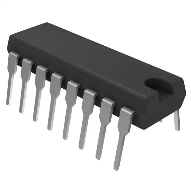
The MAX4601CPE+ is a 4-circuit SPST-NC analog switch from Analog Devices, in a 16-pin DIP package. Its 2.5 Ohm max on-resistance is the key spec for insertion loss — in a 50 Ohm system, that adds about 5% attenuation; in a high-impedance path it is negligible. The 100 mOhm channel-to-channel matching means the four switches track each other closely, which matters for differential or matched-gain stages where offset between channels would degrade common-mode rejection.
Switching speed and charge injection — timing the sample window
Turn-on time is 250 ns max, turn-off is 350 ns max. For a multiplexed ADC front-end, the 250 ns window sets the minimum acquisition time before the converter samples — the downstream op-amp must settle to the required accuracy within that interval. Charge injection is 120 pC typical; when the switch opens, that charge dumps onto the sampling capacitor, producing a voltage glitch equal to 120 pC divided by the hold capacitance. A 10 nF hold cap sees a 12 µV step; a 100 pF cap sees 1.2 V — so the charge injection spec directly governs the minimum load capacitance for a given glitch budget.
Supply flexibility — single or dual rails
In a bipolar analog system with ±15 V rails, the switch handles signals up to the rail without clipping. In a single-supply 5 V or 12 V system, the same part works without a negative rail — the signal range is from GND to V+. The 500 pA max off-leakage means the switch does not bleed charge into high-impedance nodes when it is open, preserving the voltage on a sampling cap or a photodiode bias line.
Crosstalk and channel capacitance — keeping channels isolated
Crosstalk is -59 dB at 1 MHz. That means a 1 Vpp signal on an adjacent channel couples about 1.1 mV into the switched channel at 1 MHz — acceptable for 10-bit systems but worth checking for 16-bit precision where the LSB is below 100 µV. Each channel presents 55 pF of capacitance to ground when off; in a high-frequency path, that capacitance adds to the PCB trace capacitance and lowers the bandwidth. The 1:1 multiplexer/demultiplexer circuit means each switch is a single-pole single-throw normally-closed break — no internal routing mux, just a straight pass gate.