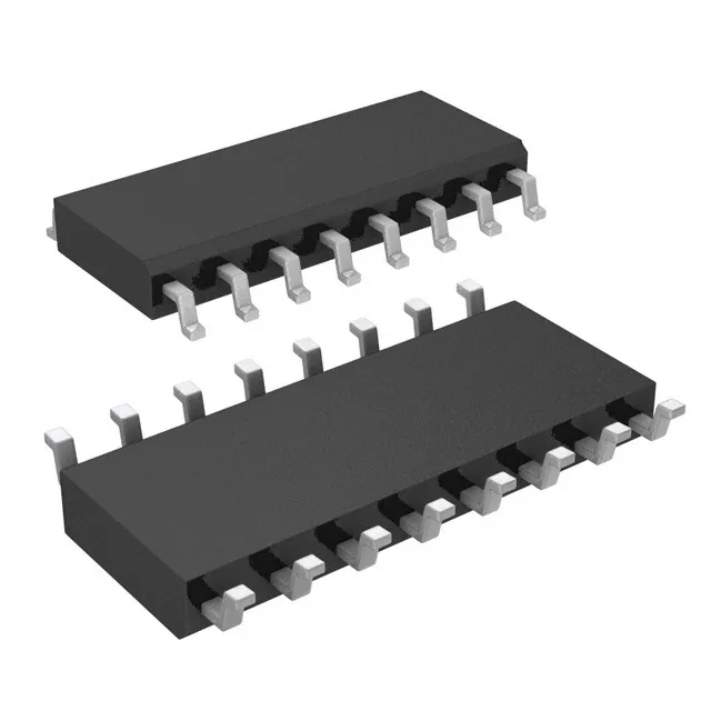
8:1 mux with dual-supply flexibility
The MAX4581CSE+: It routes one of eight input channels to a common output, or works in reverse as a demultiplexer. The part runs on either a single 2V to 12V supply or dual ±2V to ±6V rails, making it suitable for systems that need to switch signals that swing below ground. On-resistance is 80 ohms max, with channel-to-channel matching within 1 ohm. This resistance is part of the signal path, so for precision voltage measurements the load impedance should be at least 100x the mux resistance to keep the voltage divider error under 1%. The 1 ohm matching means gain errors between channels are consistent. Charge injection is 0.5 pC typical — when the mux switches channels, this charge glitch couples into the signal. For a downstream ADC with a 10 pF input capacitor, the glitch is about 50 mV, settling within the ADC's acquisition time. The -78 dB crosstalk at 1 MHz means off-channel signals leak at about 0.016% of the on-channel level — fine for 12-bit systems but worth noting for 16-bit+ designs where the noise floor is lower.
Switching speed and leakage
Turn-on time is 200 ns max, turn-off is 100 ns max. The minimum channel-to-channel switching period is 300 ns, giving a maximum channel scan rate of about 3.3 MHz. Off-channel leakage is 1 nA max at 25°C — negligible for most signal sources, but for high-impedance sensors (1 MΩ and above) the leakage creates a 1 mV offset that may need calibration. On-channel capacitance is 18 pF, off-channel capacitance is 4 pF. The 18 pF on-capacitance loads the signal source and sets the bandwidth. With a 50 Ω source impedance, the -3 dB bandwidth is about 177 MHz. The 4 pF off-capacitance contributes to the crosstalk path.
Active production and sourcing
The package is a 16-pin narrow SOIC (3.90 mm body width, 0.154" pitch), supplied in a tube. The footprint matches JEDEC MS-012. No exposed thermal pad — heat dissipation is through the leads and board copper. The commercial temperature range (0°C to 70°C) limits this variant to indoor, office, or controlled-environment use.