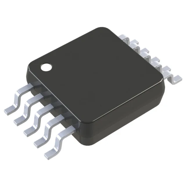
Package and footprint integration
The MAX4524EUB+: The surface-mount footprint requires a 4-layer board for clean fan-out of the signal and supply pins; a two-layer board works only if the analog traces stay short and the ground plane is continuous under the package.
Analog switching parametrics and the so-what
The SP4T 4:1 switch routes one common pin to four independent channels. The 150 Ohm max on-resistance with 2 Ohm channel-to-channel matching means the voltage drop across the switch tracks within 1.3% between channels at 1 mA signal current — this matching figure is the one that matters for gain-accuracy in a multiplexed ADC input, not the absolute R-on. Charge injection is 0.8 pC typical. For a 10 nF sample-and-hold capacitor, this injects an 80 µV glitch — negligible for a 12-bit system at 5 V reference, but it will dominate the error budget at 16 bits or above unless the acquisition window is long enough for the glitch to settle. Switching times are 150 ns turn-on and 120 ns turn-off (max). This sets the throughput ceiling: at 1 MHz scan rate, the switch spends 15% of the period settling, so the downstream ADC must wait for the full 150 ns before sampling. Off-leakage is 1 nA max. With a 100 kOhm source impedance, this leakage creates a 100 µV offset — acceptable for most industrial analog inputs but worth derating for high-impedance sensors above 1 MOhm.
Lifecycle and compliance posture
Analog Devices lists the MAX4524EUB+ as Active with ROHS3 compliance.