What the 4200 V/µs slew rate buys the signal chain
The MAX4201ESA+ is a single-channel buffer amplifier from Maxim Integrated, designed for applications that need to preserve signal edges through a unity-gain stage. Its 4200 V/µs slew rate means it can track a full-scale 2 V step in under 500 ps, making it a natural fit for driving the input of a high-speed ADC, reconstructing video waveforms, or buffering a fast DAC output without introducing slew-induced distortion. The -3 dB bandwidth of 780 MHz supports signal paths up to several hundred MHz with flat gain, so the buffer does not become the bandwidth bottleneck in an IF chain or a high-speed data converter front end. Supply current is 2.2 mA typical — low enough that in a multi-channel system you can run several buffers without a separate regulator or a big thermal via pattern.
Supply range and temperature grade — where it fits
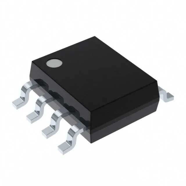
The device operates from a single supply between 8 V and 11 V, so it works directly off a 9 V or 10 V rail common in test equipment and industrial analog front ends. The -40°C to 85°C temperature range covers outdoor telecom cabinets, factory-floor instrumentation, and automotive cabin electronics without needing a mil-grade part. The 8-SOIC package (0.154" body width, 3.90 mm) is a standard footprint shared by thousands of op-amps and buffers, so layout reuse is straightforward. Surface-mount assembly with no exposed pad keeps reflow simple.
Input offset and bias — what to budget
Input offset voltage is 1 mV max, and input bias current is 800 nA. For a buffer used in a DC-coupled video path or a precision ADC driver, 1 mV of offset adds a fixed error that can be trimmed or calibrated out in software. The 800 nA bias current matters when the source impedance is high — keep the driving impedance below a few kΩ to avoid an additional offset term.
Lifecycle and sourcing posture
The MAX4201ESA+ carries an Active product status per the manufacturer, so there is no last-time-buy or end-of-life risk for new designs. ROHS3 compliant.