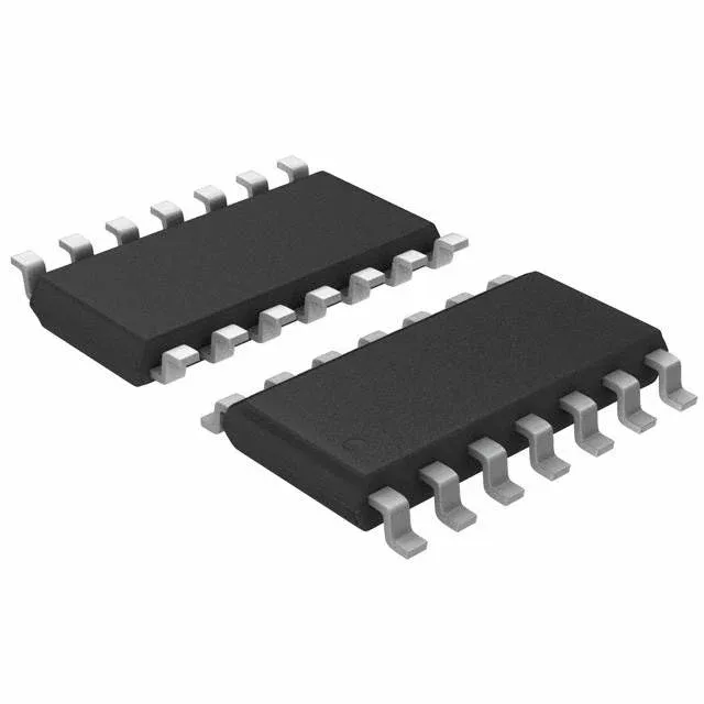
Quad SPST-NO switch for precision analog signal routing
The MAX4066CSD+T integrates four independent SPST-NO (single-pole, single-throw, normally-open) analog switches in a single 14-SOIC package, each with a 1:1 multiplexer/demultiplexer configuration. This topology is suited for routing analog or digital signals where each channel needs independent on/off control without cross-connection. Each switch presents a maximum on-resistance of 45 Ohms, with channel-to-channel matching held to 500 mOhm max — a figure that matters in gain-setting or differential signal paths where resistance mismatch introduces offset error.
Bandwidth and isolation for mixed-signal boards
The -3 dB bandwidth extends to 100 MHz, and crosstalk between channels is specified at -86 dB at 1 MHz. Together these ratings mean the switch passes a 10 MHz analog signal with under 0.1 dB of attenuation while keeping feedthrough from an adjacent channel more than 80 dB down — relevant for multiplexing video, IF, or high-speed data lines on the same IC. Switching times are 100 ns max for turn-on (Ton) and 75 ns max for turn-off (Toff), which sets the channel update rate ceiling. For a system scanning four sensor inputs, the aggregate throughput is limited by the sum of Ton plus the settling time of the downstream ADC input stage.
Charge injection and leakage in precision paths
Charge injection is rated at 1 pC typical — the amount of charge dumped onto the signal node when the switch opens. In a sample-and-hold front end driving a 16-bit ADC with a 10 nF hold capacitor, 1 pC produces a 100 µV step, which is below the 1 LSB threshold for a 5 V reference. Off-channel leakage is 1 nA max, and each channel presents 9 pF of capacitance to ground in both the on and off states.
Package, temperature grade, and compliance
Analog Devices lists this part as Active in production and ROHS3 compliant.