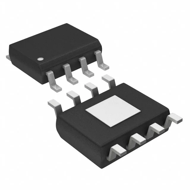
RF transistor for 836 MHz band power stages
The MAX2602ESA+ is an NPN RF transistor from Analog Devices, designed for driver and output stages in the 836 MHz cellular band. Its 11.6 dB gain at that frequency means a single stage can lift a 0 dBm input to over +11 dBm before the next stage clips — useful for GSM/EDGE power amplifier chains where every dB of stage gain saves a bias current budget. Rated 15 V collector-emitter breakdown and 1.2 A max collector current, it handles the voltage swing and peak current of a 6.4 W class-AB PA stage without collapsing the Vce margin. The 1 GHz transition frequency gives enough fT headroom for the 900 MHz band — the gain roll-off at the operating frequency stays flat.
Gain and noise figure at 836 MHz
At 836 MHz the noise figure is 3.3 dB typ — this sets the receiver front-end sensitivity floor. For a transmit driver stage the noise figure is less critical, but in a T/R switch application the same transistor sees both paths, so the 3.3 dB NF keeps the receive noise penalty under 0.5 dB when the PA is biased off. DC current gain is a minimum of 100 at 250 mA, 3 Vce — this means the base drive current stays under 2.5 mA for a 250 mA collector current, well within the range of a standard CMOS GPIO driving through a series resistor. The hFE floor at low Vce also confirms the transistor is fully saturated at the 3 V rail, not just at 5 V.
Package and thermal interface
The 150°C junction temperature rating means the die can run hot — the limiting factor is the board's ability to sink the 6.4 W through the exposed pad without exceeding the FR4 glass transition. A 2-oz copper pour under the pad with at least 12 thermal vias is the typical layout. Surface-mount assembly on standard 8-SOIC footprint — no special reflow profile beyond the standard lead-free ramp. The exposed pad requires a solder paste stencil aperture at least 50 % of the pad area to avoid voids under the die attach.
Active production and compliance
Supplied in tube packaging — 50 units per tube, ESD-safe. For reel-fed pick-and-place lines the tube can be cut and the parts bulk-loaded into a vibratory feeder or hand-placed for prototype runs.