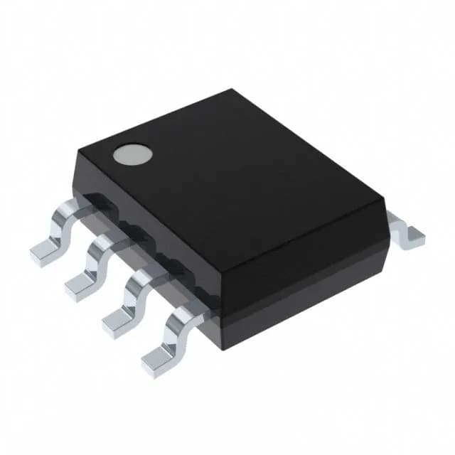
What the MAX1822ESA+ does on your board
The MAX1822ESA+ is a charge pump IC from Analog Devices that generates a positive output equal to the input voltage plus 11 V — a ratiometric boost, not a regulated rail. It takes a 3.5 V to 16.5 V input and delivers a fixed Vin+11 V output at up to 25 mA, switching at 90 kHz. The 8-SOIC package is surface-mount, rated for -40°C to +85°C operation, making it a fit for industrial and telecom bias supplies where a simple unregulated boost is acceptable.
The Vin+11V output — what it means for your rail
The fixed output of Vin+11 V means the output tracks the input with an 11 V offset.
90 kHz switching — capacitor sizing
The 90 kHz switching frequency is on the lower side for a modern charge pump, which means the external flying and output capacitors will be larger in value (typically in the microfarad range) compared to a 1 MHz part. That's a trade-off: the lower frequency reduces switching losses and radiated noise, but takes up more board area. For a bias supply on a noisy industrial rail, the quieter switching is often worth the space.
Package and rework
The 8-SOIC package is a standard Gull-wing leaded part — easy to hand-solder or rework with hot air.
Lifecycle and sourcing
The MAX1822ESA+ is listed as Active and ROHS3 compliant.