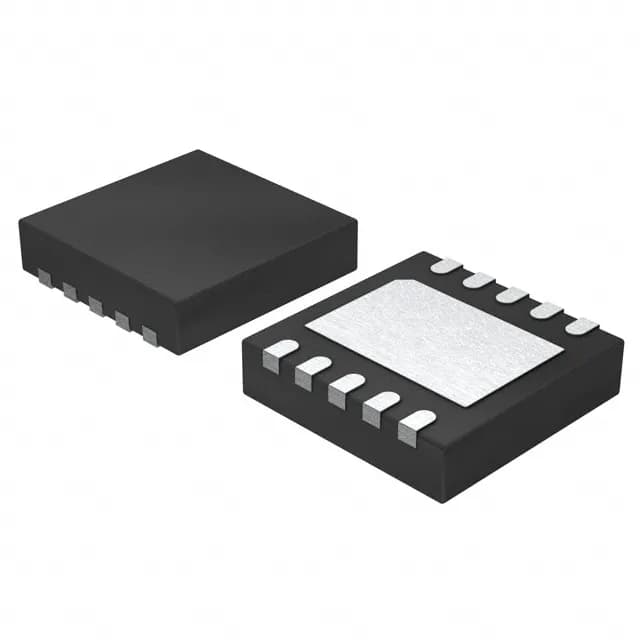
Analog Devices MAX17510ATB+T — Logic ICs

MAX17510ATB+T DDR LDO Regulator, 1.1V-3.6V Input, 10-TDFN

MPNMAX17510ATB+T
End of Life

Maxim Integrated MAX17510ATB+T, DDR LDO regulator, single output, input 1.1V~3.6V, output 0.5V~1.5V, 10-WFDFN exposed pad, -40°C~125°C, active, ROHS3.

$7.28Ref. price · indicative, final on quote
Packaging10-WFDFN Exposed Pad
StockContact for availability
MOQ1 pcs
  • 100% new & originalTraceable channels only — no refurbs, no pulls, no remarked parts.
  • Date & lot codes on quoteStated per line before you commit; label photos on request.
  • MSL-compliant ESD packingMoisture-sealed bags with indicator cards; reels photo-verified.
  • PayPal buyer protectionPay by T/T, PayPal or Payoneer — card payments covered end to end.

Specifications

MAX17510ATB+T Technical Specifications
ParameterValue
Mounting typeSurface Mount
Voltage - input1.1V ~ 3.6V
Voltage - output0.5V ~ 1.5V
Number of outputs1
Operating temperature-40°C ~ 125°C
PackageTape & Reel (TR); Cut Tape (CT)
ApplicationsLDO (Linear), DDR
Case10-WFDFN Exposed Pad

Product details

DDR termination LDO for 1.1V to 3.6V rails

The Maxim Integrated MAX17510ATB+T is a single-output LDO regulator designed specifically for DDR memory termination (VTT) applications. It accepts an input supply from 1.1V to 3.6V and delivers a programmable output from 0.5V to 1.5V, covering the termination voltages for DDR2, DDR3, DDR4, and LPDDR generations.

Input and output range — what they cover

The 1.1V to 3.6V input range is wide enough to run off a 1.2V, 1.5V, 1.8V, 2.5V, or 3.3V rail — whichever the board's core or I/O supply provides. The output adjusts from 0.5V to 1.5V, so the same part can serve as VTT for DDR3 (0.75V typical), DDR4 (0.6V typical), or LPDDR4 (0.5V to 0.6V) simply by setting the feedback divider. A single BOM line covers multiple memory interface voltages, which simplifies qualification and inventory.

Package and rework considerations

The 10-TDFN (3x3mm) with exposed pad is a common, hand-reworkable package. The pad on the bottom needs a good thermal via stitch to the ground plane — without it the junction temperature climbs fast above 300 mA continuous. The exposed pad is the main thermal path and also the ground connection; make sure the PCB footprint has a soldermask-defined opening that matches the 3x3mm land. Orientation is marked by pin 1 chamfer on the package corner — visible under a loupe after reflow.

Lifecycle and sourcing posture

No official second-source alternate is listed, but the part is a standard DDR termination LDO — the TPS51200 from TI is a functional cross-shop candidate (same class, different pinout).

Frequently asked questions

Does MAX17510ATB+T support DDR3 or DDR4 memory?

Yes. The output voltage range of 0.5V to 1.5V covers the VTT requirements for DDR3 (0.75V), DDR4 (0.6V), and LPDDR4 (0.5V to 0.6V). The input range accepts the 1.2V to 3.3V rails these memory systems typically provide.

Can MAX17510ATB+T replace TPS51200?

Both are single-output DDR termination LDOs in similar functional class, but they are not pin-compatible. The MAX17510ATB+T uses a 10-TDFN package while the TPS51200 is in a 10-MSOP or 10-VSON. A board respin would be needed to swap between them. For a drop-in replacement, check the pinout of your specific TPS51200 variant against the MAX17510 datasheet.