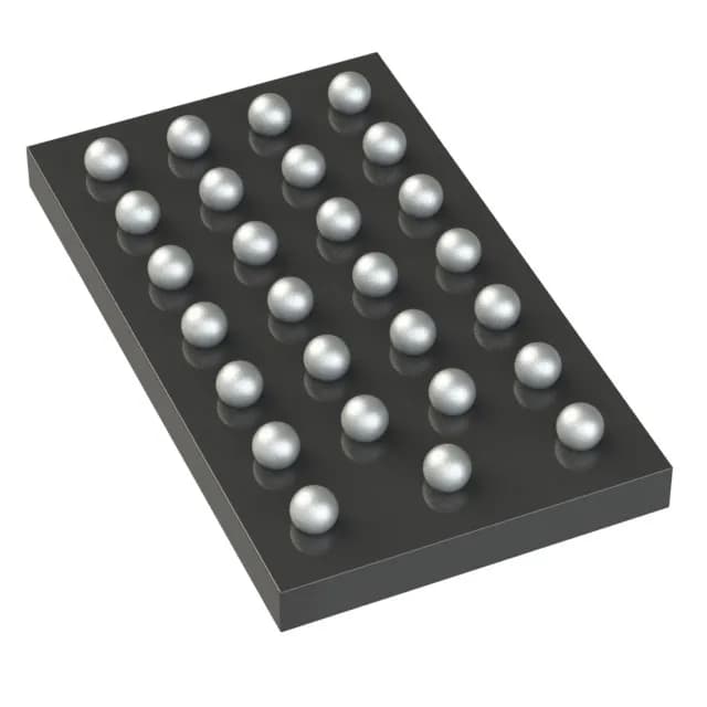
25 A in a 2.2×3.78 mm WLCSP — layout is the spec
It switches at up to 1 MHz, which lets you shrink the inductor and output capacitance, but that switching node and the 25 A loop need to be tight — the 27-WLCSP package (2.2x3.78 mm) puts the power stage right under the die, so the PCB layout and thermal via pattern are what make or break the 25 A rating.
Output voltage and switching — what to budget for
Output is adjustable from a 0.6 V minimum up to 3.3 V maximum via an external resistor divider. The 0.6 V reference is typical for modern low-voltage cores and ASIC rails. No synchronous rectifier is built in — the external Schottky diode selection matters for efficiency at high switching frequency and high current. At 1 MHz and 25 A, the diode's reverse recovery and forward drop directly affect the thermal budget.
Thermal and operating environment
That's a commercial-to-extended-industrial window — fine for most base-station, networking, and industrial equipment that lives indoors. The 25 A continuous rating assumes adequate PCB thermal management: multiple vias under the WLCSP to a ground plane, and forced airflow if ambient is near the upper end.
Lifecycle and sourcing posture
That means it's a safe selection for both prototype builds and production ramps.