3.6 A synchronous buck with a 1.4 MHz ceiling
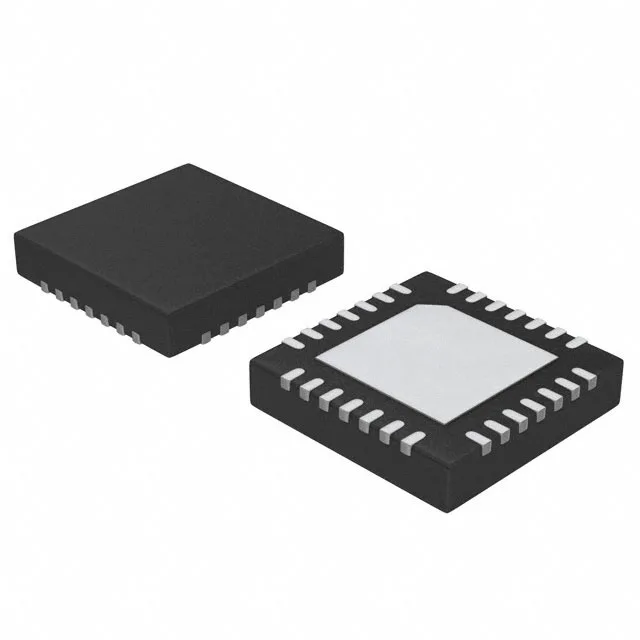
The MAX1536ETI+: Switching frequency goes up to 1.4 MHz, which lets the output inductor and capacitor shrink below the values a 500 kHz design would need. The trade-off is switching loss in the FETs — at 1.4 MHz the die runs warmer than at 300 kHz, so the thermal pad on the 28-TQFN (5x5) package needs a solid copper pour and vias to the ground plane.
Output voltage range and board-fit constraints
At 3.6 A continuous, the power dissipated in the die is roughly (Vin - Vout) × Iout × (1 - efficiency) — a 5 V to 1.8 V conversion at full load pushes about 2.5 W through the package, which requires the exposed pad to be soldered to a thermal land with at least 4 vias to the inner-layer copper. The 5.5 V input maximum means this part sits on a 5 V ±10 % rail or a lithium-ion battery (4.2 V full charge) without stress, but a 12 V intermediate bus needs a pre-regulator.