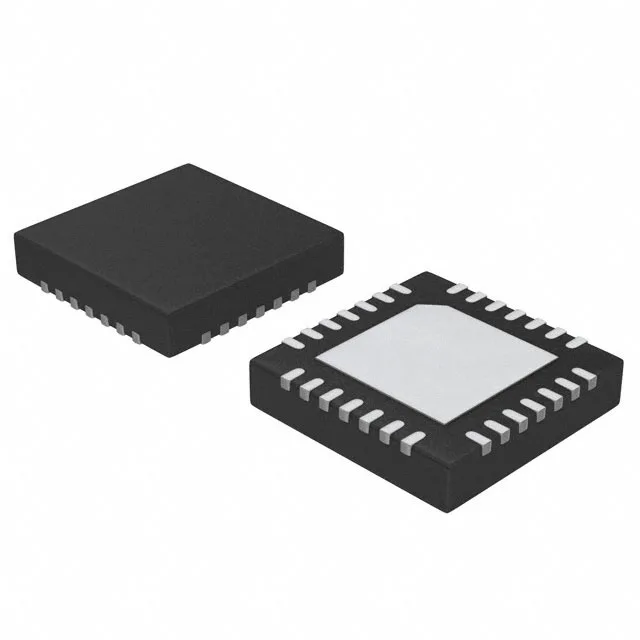
Hot swap controller with integrated 12A switch
The MAX15090BEWI+T is a single-channel hot swap controller from Analog Devices' VariableSpeed/BiLevel™ series, integrating the power MOSFET on-chip. It allows a board to be safely inserted into a live backplane without glitching the supply rail or arcing the connector pins. Rated for a continuous output current up to 12 A, it handles the inrush of a full blade server or industrial controller card without external pass transistors. The internal switch eliminates the FET selection and gate-drive layout work, but the 28-WLP package (2.07 x 3.53 mm) means the thermal path runs through the board — the copper area under the package sets the real-world current ceiling. Supply range is 2.7 V to 18 V, covering common backplane rails from 3.3 V up to 12 V. The 500 µA quiescent current is low enough to leave the controller powered continuously on the bulk supply without a meaningful standby penalty.
Programmable protection and fault handling
Six programmable functions — circuit breaker, current limit, fault timeout, overvoltage protection (OVP), slew rate, and undervoltage lockout (UVLO) — let the designer tailor the startup profile and fault response to the load capacitance and supply impedance. The slew-rate control ramps the output voltage, limiting inrush current to a value set by the external capacitor. On a fault, the latched fault response holds the switch off until the input is cycled or the enable is toggled — no auto-retry, which is the safer choice for a board that could arc if power is re-applied into a short. The thermal-limit feature protects the die if the junction temperature climbs above the safe operating area. The controller itself draws 500 µA from the input rail, so self-heating is negligible; the die temperature is dominated by the I²R loss of the internal switch at the load current.
Package, footprint, and compliance
Housed in a 28-bump WFBGA (WLBGA) package, the MAX15090BEWI+T is a true chip-scale device — the 2.07 x 3.53 mm footprint saves board area but requires a solder-mask-defined pad and a via-in-pad layout for the centre bumps that carry the load current. The bump pitch is fine enough that a 4-layer PCB with microvias is the practical minimum for a 12 A design. Surface-mount assembly only; the tape-and-reel packaging (also available in cut tape) feeds standard pick-and-place lines. The device is ROHS3 compliant, with no exemptions for lead or other restricted substances.