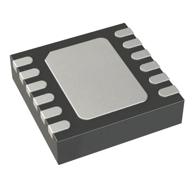
The MAX14839GTC+T comes in a 12-WFDFN exposed pad package, 3x3 mm footprint (12-TDFN). Supply current is 1.2 mA typical. That is the load the part draws from the upstream logic rail — low enough for an always-on block in a power-sensitive design, but not micro-power for a battery node that sleeps for months. Operating temperature range is -40°C to 105°C. The temp grade alone tells you the silicon is rated for the thermal profile of a motor-drive cabinet or an outdoor telecom shelf.
What the logic-level interface means for the BOM
Both input and output are logic-level — the part is a digital output driver, not an analog buffer or a level translator with a separate supply rail. The input type is Logic, output type is Logic. That means it accepts a standard CMOS or TTL-level signal and drives a logic-level load. If your BOM line expects an analog output or a high-current gate driver, this is not the part. The part is classified as an Output Driver in the Discrete Semiconductors category. That places it alongside line drivers, peripheral drivers, and relay drivers — not general-purpose logic gates or buffers. The function is to take a logic input and drive a load that needs more fan-out or a cleaner edge than a standard logic output provides.
If you need a drop-in alternate for a dual-source BOM strategy, the pinout and function are specific to this ADI part. A functional equivalent would require a board spin.