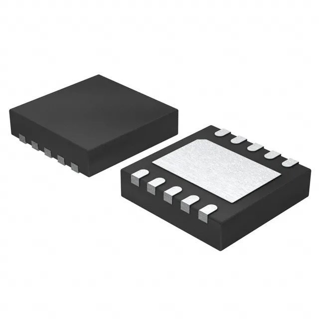
Analog Devices MAX14761ETB+T — Discrete Semiconductors

MAX14761ETB+T Analog Devices SPST Switch, 2Ohm, 10-TDFN

MPNMAX14761ETB+T
End of Life

Analog Devices MAX14761ETB+T SPST-NO/NC analog switch, dual 2:1 mux, 2 Ohm on-resistance, -83dB crosstalk at 100kHz, 10-TDFN (3x3) package, Tape & Reel.

$7.4Ref. price · indicative, final on quote
Packaging10-WFDFN Exposed Pad
StockContact for availability
Lead timeIn Stock wk
MOQ1 pcs
  • 100% new & originalTraceable channels only — no refurbs, no pulls, no remarked parts.
  • Date & lot codes on quoteStated per line before you commit; label photos on request.
  • MSL-compliant ESD packingMoisture-sealed bags with indicator cards; reels photo-verified.
  • PayPal buyer protectionPay by T/T, PayPal or Payoneer — card payments covered end to end.

Specifications

MAX14761ETB+T Technical Specifications
ParameterValue
Mounting typeSurface Mount
Voltage - supply, single (V+)3V ~ 5.5V
Current - leakage (IS(off))250nA
Operating temperature-40°C ~ 85°C (TA)
-3db bandwidth100MHz
PackageTape & Reel (TR); Cut Tape (CT)
Crosstalk-83dB @ 100kHz
Case10-WFDFN Exposed Pad
Switch circuitSPST - NO/NC
Charge injection1370pC
Number of circuits2
On-State resistance2Ohm
Switch time (Ton, toff)300µs, 1ns
Multiplexer (Demultiplexer circuit)1:1
Channel-to-Channel matching (ΔRon)5.1mOhm

Product details

Dual SPST switch with low on-resistance and high isolation

The MAX14761ETB+T is a dual 1:1 multiplexer/demultiplexer from Analog Devices, configured as two independent SPST switches — one normally-open, one normally-closed per the SPST - NO/NC topology. Each switch carries a maximum on-resistance of 2 Ohm, with channel-to-channel matching held to 5.1 mOhm, so the insertion loss across the two paths tracks tightly in a differential signal chain. The -3 dB bandwidth is 100 MHz, and crosstalk between channels is -83 dB at 100 kHz — this combination suits the part for routing audio or low-speed data signals where isolation between adjacent paths matters more than raw switching speed.

Signal integrity and parametric boundaries

Maximum switch times are 300 µs for turn-on and 1 ns for turn-off — the asymmetric timing means the off-to-on transition is the bottleneck for multiplexing applications; the fast turn-off prevents glitch feedthrough when the control signal drops. Charge injection is 1370 pC, a figure to budget for in sample-and-hold or precision integrator front-ends where the injected charge appears as a step on the hold capacitor. Off-state leakage is 250 nA max at 25 °C — in a high-impedance node this leakage current multiplied by the source impedance produces an offset error that may dominate the signal chain budget.

Package, footprint, and temperature grade

The 3x3 mm body with 0.50 mm pitch is a common DFN footprint; the stencil aperture for the centre pad should be segmented to avoid solder voiding during reflow. Surface-mount only; the Tape & Reel (TR) and Cut Tape (CT) options suit both prototype and production volumes.

Lifecycle and compliance posture

Analog Devices lists the MAX14761ETB+T as Active (current production) and ROHS3 Compliant.

Frequently asked questions

How do I get current pricing and availability for MAX14761ETB+T?

Pricing and availability are confirmed at quote time against your BOM quantity. Submit an RFQ through this listing; the storefront sources through independent distribution channels and returns a firm quote with lead time.

What is the crosstalk specification for MAX14761ETB+T?

Crosstalk is -83 dB at 100 kHz. The -3 dB bandwidth is 100 MHz, so the isolation holds well into the low-MHz range before rolling off.