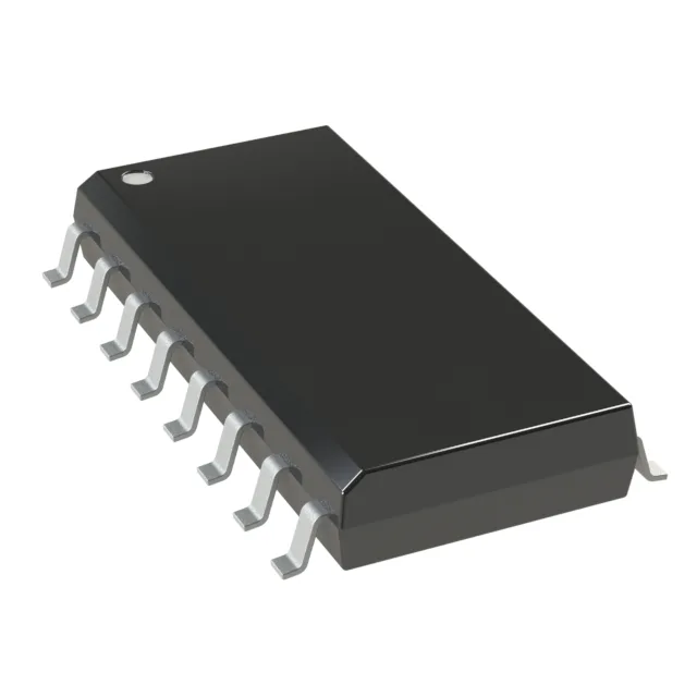
Dual SP4T switch with wide supply range
The MAX14753EUE+T is a dual SP4T (single-pole, four-throw) analog switch from Analog Devices, configured as two independent 4:1 multiplexer/demultiplexer circuits in a single 16-TSSOP package. Each switch path presents a maximum on-resistance of 130 Ohm, with channel-to-channel matching held to 500 mOhm — tight enough to keep gain errors consistent across multiplexed channels in a precision analog front-end. The part accepts a single supply from 20 V to 72 V, or dual supplies from ±10 V to ±36 V, covering common industrial bipolar rails (±15 V, ±24 V) and unipolar high-voltage buses (48 V, 60 V). This supply flexibility lets the switch handle large signal swings without clipping — a key requirement when multiplexing ±10 V sensor outputs or ±15 V data acquisition signals.
Crosstalk and charge injection in the signal chain
Crosstalk is specified at -62 dB at 100 kHz — this is the isolation between channels when one is active and the other is off. For a 16-bit ADC with a 100 kHz sampling rate, -62 dB of feedthrough keeps the interference from an adjacent channel below 0.5 LSB, assuming full-scale signals. If your multiplexer sits ahead of a high-resolution converter, this spec determines whether the off-channel leakage swamps the measurement. Charge injection is 200 pC typical — the amount of charge dumped onto the signal line when the switch turns off. In a sample-and-hold front-end, this charge creates a voltage step across the hold capacitor; for a 10 nF cap, 200 pC produces a 20 µV glitch. The -3 dB bandwidth of 20 MHz means the switch settles fast enough for most audio and low-speed instrumentation paths, but the charge injection floor sets the practical resolution limit in precision DC applications. Leakage current is 20 nA max per switch in the off state. For a 10 MΩ source impedance, 200 nA translates to a 2 mV offset error — worth derating if your signal source is high-impedance.
Package and board integration
The 16-TSSOP footprint is a standard JEDEC outline, so the PCB layout matches any generic TSSOP-16 land pattern. No exposed pad — thermal management relies on the copper traces and the ambient airflow, adequate for the sub-milliamp quiescent current of a CMOS switch. Switching times are 25 µs max on and 2 µs max off — the asymmetric timing means the break-before-make interval is dominated by the turn-off time. In multiplexer applications, this guarantees the previous channel is fully disconnected before the next one connects, preventing momentary short circuits between signal sources.