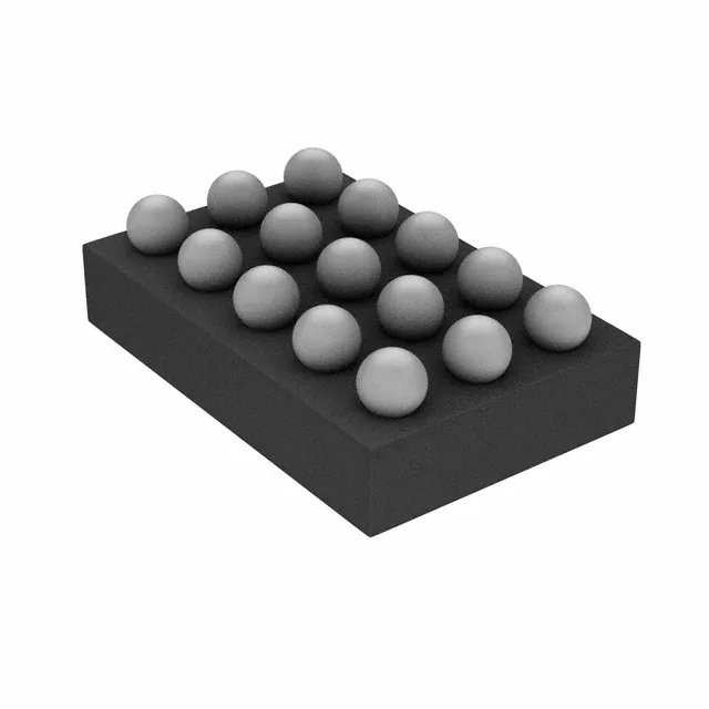
6A high-side switch in a 1.22x2.05mm WLP
The MAX14713EWL+T: This is a single-output, high-side power switch with a 2:1 input-to-output ratio — two input voltage sources can be multiplexed to one output rail under logic control via the On/Off interface. The 11mOhm typical Rds(on) keeps conduction loss at 6A to roughly 400mW, but the real thermal limit is set by the 15-WLP package's junction-to-board thermal resistance, not the silicon itself.
15-WLP layout considerations
The 15-WLP (1.22x2.05mm) package uses a fine-pitch BGA array — the supplier device package designation 15-WLP (1.22x2.05) indicates the die-scale footprint. Solder paste volume and stencil aperture must be controlled to avoid bridging between adjacent bumps; a 0.4mm pitch is typical for this class of WLP. The board-side copper pad pattern should match the recommended land pattern from the datasheet, with thermal vias under the package to pull heat into the PCB ground plane. Surface-mount assembly with standard reflow profiles works, but the WLP's exposed backside is the die itself — no mold compound overhang. The package is moisture-sensitive; bake before reflow if the floor life has been exceeded per the MSL label on the reel.