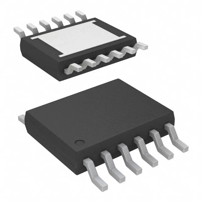
Half-Bridge Driver in a 12-TSSOP Exposed Pad
The LTC7060EMSE#WPBF is a half-bridge gate driver from Analog Devices, configured as two outputs (half-bridge topology) with a 6 A peak drive current per channel. The 12-TSSOP package with exposed pad (12-MSOP-EP) requires a thermal land pattern on the PCB — the copper pour and via array under the pad must handle the conduction loss from the 800 mOhm LS / 1.5 Ohm HS typical Rds(on) at full load. The supply and load voltage range is 6 V to 14 V, a narrow window suited for 12 V intermediate bus architectures or battery-powered systems. The PWM interface accepts a single input; the driver's internal dead-time and shoot-through protection prevent cross-conduction during the switching transition.
6 A Peak Drive and Bootstrap Circuit
Each channel delivers 6 A peak output, sufficient to drive the gate charge of medium-power MOSFETs in a half-bridge. The bootstrap circuit generates the high-side supply voltage from the low-side rail — the bootstrap capacitor must be sized for the gate charge of the chosen FETs and the switching frequency. The UVLO fault protection holds the outputs low until the supply voltage rises above the threshold, preventing the MOSFETs from operating in the linear region during startup or brownout. The shoot-through protection enforces a minimum dead-time between high-side and low-side turn-on.
Active Lifecycle and ROHS3 Compliance
ROHS3 compliant — the solder termination finish and package materials meet the EU RoHS exemption-free standard. The -40°C to 150°C junction temperature range covers industrial and automotive under-hood thermal environments, though the 150°C Tj(max) is the hard limit for the exposed-pad thermal design.