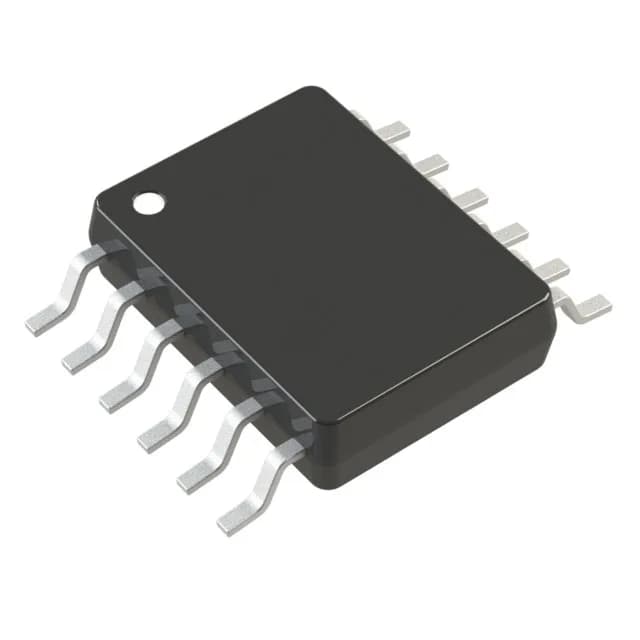
Analog Devices LTC6957IMS-2#PBF — Clock & Timing ICs

LTC6957IMS-2#PBF Clock Fanout Buffer, LVDS Output, 300 MHz

MPNLTC6957IMS-2#PBF
End of Life

Analog Devices LTC6957IMS-2#PBF, Fanout Buffer (Distribution), 1:2 LVDS output, 300 MHz max, 3.15V~3.45V supply, -40°C~85°C, 12-MSOP, Tube, ROHS3 compliant.

$10.82Ref. price · indicative, final on quote
Packaging12-TSSOP (0.118", 3.00mm Width)
StockContact for availability
MOQ1 pcs
  • 100% new & originalTraceable channels only — no refurbs, no pulls, no remarked parts.
  • Date & lot codes on quoteStated per line before you commit; label photos on request.
  • MSL-compliant ESD packingMoisture-sealed bags with indicator cards; reels photo-verified.
  • PayPal buyer protectionPay by T/T, PayPal or Payoneer — card payments covered end to end.

Specifications

LTC6957IMS-2#PBF Technical Specifications
ParameterValue
TypeFanout Buffer (Distribution)
Mounting typeSurface Mount
Voltage3.15V ~ 3.45V
Frequency300 MHz
Operating temperature-40°C ~ 85°C
InputCML, CMOS, LVDS, LVPECL
OutputLVDS
PackageTube
Case12-TSSOP (0.118\", 3.00mm Width)
Number of circuits1
Ratio - Input:Output1:2
Differential - Input:OutputYes/Yes

Product details

What this clock buffer does on your board

The LTC6957IMS-2#PBF is a 1:2 fanout buffer that takes a single-ended or differential clock input and delivers two LVDS output copies. It accepts CML, CMOS, LVDS, or LVPECL input signals, making it a flexible clean-up stage for clock trees that need to drive multiple loads without degrading edge rates. Maximum frequency is 300 MHz, which covers most baseband, ADC/DAC reference, and FPGA reference clock distribution. The differential input-to-output path means the buffer preserves signal integrity for high-speed links.

Supply and temperature range

Supply voltage is tightly regulated at 3.15 V to 3.45 V — this is a 3.3 V nominal rail with ±0.15 V tolerance.

Active production — no end-of-life watch needed

Sourced per RFQ against your BOM quantity — confirm the package variant (12-MSOP, tube) matches your assembly line's feeder setup.

Frequently asked questions

What output does LTC6957IMS-2#PBF provide?

It provides two LVDS output copies (1:2 fanout). The LVDS output is differential, which helps maintain signal integrity over short PCB traces to downstream PLLs, FPGAs, or ADCs.

Can LTC6957IMS-2#PBF accept a 3.3V CMOS input?

Yes, the input stage accepts CMOS signals alongside CML, LVDS, and LVPECL. The supply voltage range of 3.15 V to 3.45 V means a 3.3 V CMOS input is within the common-mode range for the differential receiver.

What is the difference between LTC6957IMS-1#PBF and LTC6957IMS-2#PBF?

The LTC6957IMS-1#PBF provides LVPECL outputs, while the LTC6957IMS-2#PBF provides LVDS outputs. Both share the same 300 MHz bandwidth, input flexibility, and 12-MSOP package. Choose the output logic family that matches your downstream load — LVDS for lower swing and reduced power, LVPECL for higher edge rates.