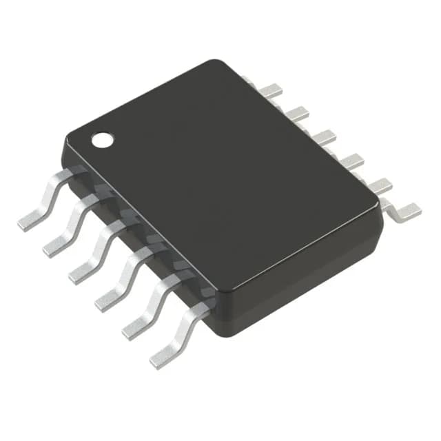
What is this part and where does it fit?
The LTC6957HMS-1#PBF is a 1:2 fanout buffer from Analog Devices that takes one differential or single-ended clock input and delivers two LVPECL outputs. It handles up to 300 MHz and accepts CML, CMOS, LVDS, or LVPECL inputs, so it bridges between different logic families on a clock tree. The 3.15V–3.45V supply rail is tight—plan for a clean 3.3V rail with ±5% regulation.
The 300 MHz maximum frequency sets the speed ceiling for clock distribution. If your system runs a 200 MHz reference, this buffer has margin; at 300 MHz you are at the limit, so check the output rise/fall times against your receiver setup/hold. Input accepts CML, CMOS, LVDS, and LVPECL—this is the main flexibility win. A single BOM line can handle a CMOS oscillator on one build and an LVDS PLL output on another, as long as the output is LVPECL. The 1:2 fanout ratio means one input drives two loads; for more than two outputs, cascade another buffer or use a 1:4 part. The 12-TSSOP package (0.118" wide, 3.00 mm) with 0.65 mm pitch fits on a 2-layer board but benefits from a ground plane under the part for signal integrity at high frequencies. The MSOP-12 footprint is shared with other LTC6957 variants, so a layout can be reused across output types.
Lifecycle and supply posture
ROHS3 compliant (Pb-free). Sourced to order against your BOM quantity; no stock-holding claim, confirmed per RFQ.