What this PLL clock synthesizer does
The LTC6951IUHF#PBF is a single-circuit PLL clock synthesizer that accepts a clock input and produces up to five outputs in CML or LVDS format, with a maximum output frequency of 2.5 GHz. This makes it a fit for high-speed ADC/DAC clocking, SERDES reference generation, or RF LO synthesis in test equipment and base station infrastructure.
Supply rail and temperature grade
The supply range is 3.15V to 3.45V, so a nominal 3.3V rail sits comfortably inside the window. The industrial temperature grade of -40°C to 105°C supports outdoor and under-hood deployment without a commercial-grade derating step.
Package and rework considerations
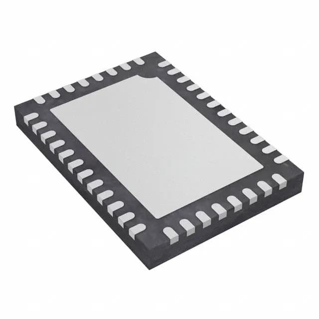
Housed in a 40-WFQFN with exposed pad (5x7 mm body), the part has a central thermal pad that must be soldered to a ground plane with thermal vias. The exposed pad also serves as the low-inductance return path for the PLL charge pump — a cold solder joint under the pad will degrade phase noise.