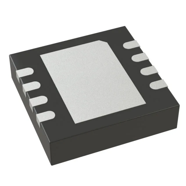
Analog Devices LTC6244CDD#TRPBF — Microcontrollers & Processors (MCU / MPU / DSP)

LTC6244CDD#TRPBF CMOS Op-Amp, 50 MHz, 35 V/µs

MPNLTC6244CDD#TRPBF
End of Life

Analog Devices LTC6244CDD#TRPBF CMOS dual op-amp, 50 MHz gain bandwidth, 35 V/µs slew rate, rail-to-rail output, 8-DFN (3x3) package, Tape & Reel.

$5.38Ref. price · indicative, final on quote
Packaging8-WFDFN Exposed Pad
StockContact for availability
Lead timeIn Stock wk
MOQ1 pcs
  • 100% new & originalTraceable channels only — no refurbs, no pulls, no remarked parts.
  • Date & lot codes on quoteStated per line before you commit; label photos on request.
  • MSL-compliant ESD packingMoisture-sealed bags with indicator cards; reels photo-verified.
  • PayPal buyer protectionPay by T/T, PayPal or Payoneer — card payments covered end to end.

Specifications

LTC6244CDD#TRPBF Technical Specifications
ParameterValue
Output typeRail-to-Rail
Mounting typeSurface Mount
Amplifier typeCMOS
Voltage - input offset100 µV
Voltage - supply span2.8 V
Current - supply6.25mA (x2 Channels)
Current - input bias1 pA
Current - output (Channel)35 mA
Operating temperature0°C ~ 70°C
Gain bandwidth product50 MHz
PackageTape & Reel (TR); Cut Tape (CT)
Slew rate35V/µs
Case8-WFDFN Exposed Pad
Number of circuits2

Product details

Signal-chain fit for a 50 MHz rail-to-rail CMOS op-amp

The LTC6244CDD#TRPBF is a dual CMOS operational amplifier from Analog Devices, packing 50 MHz gain-bandwidth product and a 35 V/µs slew rate into an 8-DFN (3x3) package. The rail-to-rail output stage lets it swing to within millivolts of the supply rails, so it can drive an ADC input or a comparator threshold without an extra level-shift stage. With 1 pA typical input bias current, it suits high-impedance sensor front-ends where the bias current error would otherwise dominate the offset budget.

Parametric depth: what the ratings mean for the BOM

The 50 MHz gain-bandwidth product sets the closed-loop bandwidth ceiling — at a noise gain of 10, the usable -3 dB bandwidth is about 5 MHz, which covers fast sensor conditioning or a photodiode transimpedance stage. Each channel draws 6.25 mA quiescent current — the total 12.5 mA for both amplifiers is about 63 mW at 5 V, which is moderate for a 50 MHz part but worth budgeting in a thermally constrained enclosure. Input offset voltage is 100 µV typical, and each channel can deliver 35 mA output current. The CMOS input stage keeps bias current at 1 pA typical, which is the key spec for a pH probe or a precision current-sense amplifier where the source impedance is in the megohm range.

Package and board integration

The 0.5 mm pitch DFN footprint is manageable on a two-layer board if the fan-out traces are kept short; a four-layer stack-up with a dedicated ground plane under the paddle is cleaner for high-frequency signal integrity.

Frequently asked questions

What is the closest functional second-source for LTC6244CDD#TRPBF?

The AD8652ARZ-REEL7 is a parametric peer from the same Analog Devices DigiTrim® family — it offers 50 MHz GBW, 41 V/µs slew rate, 1 pA input bias, and rail-to-rail CMOS output in a similar dual-channel configuration. The LTC6244 runs on a 2.8-6 V supply, while the AD8652 operates from 2.7-5.5 V.

What is LTC6244CDD#TRPBF's slew rate and what does it mean for my design?

The slew rate is 35 V/µs typical. This means the output can change 1 V in about 28 ns, which is fast enough to handle a 2 Vpp sine wave at 5 MHz without slewing distortion. For a pulse or square-wave application, the rise time into a capacitive load will be slower — budget the output current limit (35 mA per channel) when driving a heavy load.