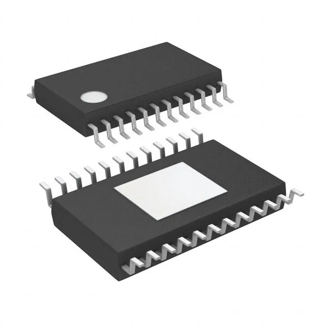
Analog Devices LTC3618IFE#PBF — Discrete Semiconductors

LTC3618IFE#PBF DDR Converter, 2.25-5.5V Input, 24-TSSOP

MPNLTC3618IFE#PBF
End of Life

Analog Devices LTC3618IFE#PBF DDR Converter IC, 2.25V to 5.5V input, 2 outputs, adjustable to 0.6V, -40°C to 125°C, 24-TSSOP exposed pad, Tube.

$11.9Ref. price · indicative, final on quote
Packaging24-TSSOP (0.173", 4.40mm Width) Exposed Pad
StockContact for availability
Lead timeIn Stock wk
MOQ1 pcs
  • 100% new & originalTraceable channels only — no refurbs, no pulls, no remarked parts.
  • Date & lot codes on quoteStated per line before you commit; label photos on request.
  • MSL-compliant ESD packingMoisture-sealed bags with indicator cards; reels photo-verified.
  • PayPal buyer protectionPay by T/T, PayPal or Payoneer — card payments covered end to end.

Specifications

LTC3618IFE#PBF Technical Specifications
ParameterValue
Mounting typeSurface Mount
Voltage - input2.25V ~ 5.5V
Voltage - outputAdj to 0.6V
Number of outputs2
Operating temperature-40°C ~ 125°C
PackageTube
ApplicationsConverter, DDR
Case24-TSSOP (0.173\", 4.40mm Width) Exposed Pad

Product details

DDR termination regulator in a 24-TSSOP exposed pad package

The LTC3618IFE#PBF is a DDR converter IC from Analog Devices designed specifically for DDR memory termination and tracking applications. It delivers two regulated outputs from an input range of 2.25V to 5.5V, making it compatible with both 2.5V and 5V rails common in DDR VDDQ supplies. The first output provides the VTT termination voltage, adjustable down to 0.6V, while the second output generates the VREF reference voltage. This dual-output architecture is standard for DDR1 through DDR4 memory systems where tight tracking between VTT and VREF is critical for signal integrity on the data bus.

Industrial temperature grade and package fit

Rated for -40°C to 125°C operating temperature, the LTC3618IFE#PBF is suited for industrial environments where ambient temperatures exceed commercial limits. The 24-TSSOP package with exposed pad (0.173" body width, 4.40mm) requires a thermal land pattern on the PCB to dissipate heat from the internal power FETs — the exposed paddle must be soldered to a copper plane for rated output current. The adjustable output down to 0.6V covers the VTT termination voltage for DDR3 (0.75V) and DDR4 (0.6V) standards. The input range from 2.25V to 5.5V means a single 3.3V or 5V rail can supply both the VDDQ and the converter, simplifying the power tree on a memory module or motherboard.

Frequently asked questions

Is LTC3618IFE#PBF compatible with 2.5V and 5V inputs?

Yes. The input voltage range is 2.25V to 5.5V, so it operates directly from 2.5V and 5V rails without additional regulation. This covers DDR VDDQ supplies at both voltage levels.