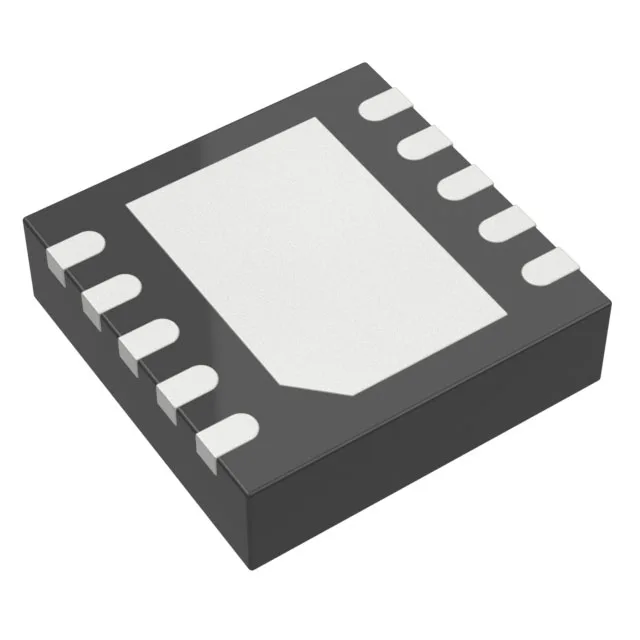
10-DFN package with exposed pad — the board-level integration story
The LTC3422EDD#PBF comes in a 10-lead WFDFN with an exposed pad (3×3 mm footprint). That pad is the primary thermal path — it must be soldered to a copper plane on the PCB to keep the junction temperature within the -40 to +85 °C operating range under load. The 0.5 mm pitch demands a well-planned fan-out; the inner pins connect to the pad via short traces to minimise parasitic inductance in the switching loop.
0.5 V to 4.5 V input, 1.5 A switch — what the boost rating means for your rail
This is a synchronous step-up converter that starts from an input as low as 0.5 V — think single-cell alkaline or Li-ion that has discharged deep. The internal switch is rated for 1.5 A peak current; that figure sets the maximum output power before the switch current limit engages. At a 3.3 V output from a 1.8 V input, the switch duty cycle is about 45 %, and the 1.5 A limit translates to roughly 900 mA output before foldback — assuming reasonable inductor selection and layout. The synchronous rectifier (the low-side MOSFET replaced by a switch) improves efficiency at lower output voltages compared to a diode-based boost. At 2.5 V out, the voltage drop across a Schottky would eat 10-15 % of the output; the synchronous FET keeps that loss to the Rds(on) times the inductor current.
100 kHz to 3 MHz switching frequency — size vs. efficiency trade-off
The switching frequency is programmable from 100 kHz to 3 MHz via a resistor on the RT pin. Lower frequencies (100-300 kHz) give better efficiency because switching losses scale with frequency, but require larger inductors and output capacitors. At 3 MHz the external components shrink to 0603 or 0805 sizes — useful for space-constrained designs — but the efficiency drops by 5-8 % depending on load. The frequency also sets the output ripple; at 3 MHz the ripple amplitude is lower for the same output capacitance, which helps in noise-sensitive loads.
Adjustable output from 2.25 V to 5.25 V — the feedback divider sets the rail
The output is adjustable via an external resistor divider from a 0.6 V internal reference. The minimum output is 2.25 V (the reference plus headroom for the error amplifier), and the maximum is 5.25 V — limited by the absolute maximum rating of the output pin. For a 3.3 V rail, a standard 1% divider with 10 kΩ upper and 4.42 kΩ lower resistor works. The single-output configuration means one feedback network per converter.
Active production, RoHS3 — sourcing posture
The LTC3422EDD#PBF carries an active lifecycle status from Analog Devices. It is RoHS3 compliant (lead-free, no exemptions). Sourced through independent distribution channels; quoted to order against BOM quantities. No official second-source or pin-compatible alternative is recorded — the 10-DFN package and pinout are unique to this part within the LTC3422 family.