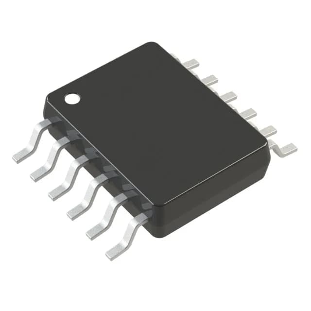
Dual 12-bit PWM DAC with extended temperature range
It integrates two DAC channels in a 12-MSOP package, each with its own PWM demodulator and output buffer, so a single PWM signal per channel generates a clean analog voltage without an external filter.
The data interface is PWM, not SPI or I2C. That is the defining difference versus most precision DACs: you feed a variable-duty-cycle digital signal on each channel's PWM input, and the internal demodulator converts it to a DC voltage. The settling time to 0.5 LSB is 7.8 µs typ, which sets the minimum PWM period you can use. If your PWM carrier runs at, say, 1 kHz (1 ms period), the DAC settles well within one cycle. At higher PWM frequencies — 100 kHz gives a 10 µs period — the 7.8 µs settling consumes most of the period, so the output may not fully settle before the next update. For closed-loop applications, budget the settling time against your PWM update rate.
Accuracy budget: ±1 LSB INL and DNL
Integral and differential nonlinearity are both specified at ±1 LSB maximum at 12 bits. That means every code is guaranteed monotonic, and the worst-case deviation from an ideal transfer function is one LSB — about 0.024% of full scale at 5 V reference. No calibration is needed for most 12-bit systems; if your error budget allocates ±0.1% for the DAC, this part fits without trimming. The reference can be external or internal, so you can match the full-scale range to the ADC reference or sensor output span.
Package and supply: 12-MSOP footprint, single-supply operation
Housed in a 12-MSOP (3.00 mm × 3.00 mm body, 0.65 mm pitch), this DAC fits on dense mixed-signal boards where every mm² counts. The output is rail-to-rail buffered, swinging from near ground to within a few millivolts of the positive rail. Surface-mount assembly is standard; no exposed pad to route.
Lifecycle and sourcing
For volume commitments or scheduled deliveries, a procurement inquiry will establish lead time and price breaks.