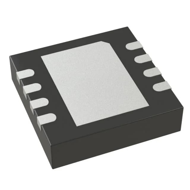
Analog Devices LTC2641CDD-16#PBF — DC-DC Power Modules

LTC2641CDD-16#PBF 16-Bit DAC, SPI, 1µs, 8-DFN

MPNLTC2641CDD-16#PBF
End of Life

Linear Technology LTC2641CDD-16#PBF, 16-bit voltage-output DAC, R-2R architecture, SPI interface, 1µs settling time, ±0.5 LSB INL/DNL, single channel, external reference, 2.7V-5.5V supply, 8-DFN (3x3) package, 0°C to 70°C.

$15.76Ref. price · indicative, final on quote
Packaging8-WFDFN Exposed Pad
StockContact for availability
MOQ1 pcs
  • 100% new & originalTraceable channels only — no refurbs, no pulls, no remarked parts.
  • Date & lot codes on quoteStated per line before you commit; label photos on request.
  • MSL-compliant ESD packingMoisture-sealed bags with indicator cards; reels photo-verified.
  • PayPal buyer protectionPay by T/T, PayPal or Payoneer — card payments covered end to end.

Specifications

LTC2641CDD-16#PBF Technical Specifications
ParameterValue
Output typeVoltage - Unbuffered
Mounting typeSurface Mount
Reference typeExternal
Voltage - supply, analog2.7V ~ 5.5V
Voltage - supply, digital2.7V ~ 5.5V
InterfaceSPI
Operating temperature0°C ~ 70°C
PackageTube
ArchitectureR-2R
INL (DNL)±0.5, ±0.5
Settling time1µs (Typ)
Number of bits16
Case8-WFDFN Exposed Pad
Differential outputNo
Number of d (A converters)1

Product details

16-bit precision DAC for single-channel voltage output

The Linear Technology LTC2641CDD-16#PBF is a single-channel, 16-bit voltage-output digital-to-analog converter using an R-2R ladder architecture. It delivers ±0.5 LSB INL and ±0.5 LSB DNL, settling to 1 LSB within 1 µs typical. The SPI data interface accepts update commands at clock rates limited only by the host controller. An external voltage reference sets the full-scale output range, giving the designer control over the span independent of the supply rails. Supply range is 2.7 V to 5.5 V for both analog and digital sections, simplifying single-rail designs. The part is packaged in an 8-lead WFDFN with exposed pad (3 mm × 3 mm) for surface-mount assembly.

What the ±0.5 LSB linearity means for your BOM

The ±0.5 LSB INL and DNL guarantee monotonic behavior across the full 16-bit code range. No missing codes, no non-monotonic steps. That matters when the DAC is driving a closed-loop actuator or setting a precision threshold — the output voltage moves predictably with each code increment. The 1 µs settling time supports update rates up to roughly 1 Msps in a sample-and-hold application, though the SPI bus speed and host overhead will be the real limit. For a BOM line that needs a clean 16-bit voltage output without external buffer or level shift, this part covers the analog path from the serial interface to the output pin.

Commercial temperature grade — design-in boundary

The operating temperature range is 0°C to 70°C. The AD5541ARZ peer is rated from -40°C to 125°C.

Lifecycle and supply position

Status is Active per the manufacturer, with ROHS3 compliance. For dual-sourcing consideration, the AD5541ARZ is a functional equivalent with the same R-2R core, 16-bit resolution, ±0.5 LSB linearity, and 1 µs settling, but in an SOIC-8 package and rated for -40°C to 125°C.

Frequently asked questions

What is the resolution of LTC2641CDD-16#PBF?

It is a 16-bit DAC. The ±0.5 LSB INL and DNL mean the effective resolution equals the full 16 bits — no missing codes, monotonic over the entire range.

What is the equivalent of LTC2641CDD-16#PBF?

The AD5541ARZ is a functional equivalent: same R-2R architecture, 16-bit resolution, ±0.5 LSB INL/DNL, 1 µs settling, and SPI interface. The key difference is the AD5541ARZ operates from -40°C to 125°C and comes in an SOIC-8 package — not pin-compatible with the 8-DFN footprint of the LTC2641CDD-16#PBF.

What is the output type of LTC2641CDD-16#PBF?

Voltage output, unbuffered. The R-2R ladder drives the output pin directly. An external reference sets the full-scale voltage. The output impedance is code-dependent, so a buffer amplifier is recommended if driving a low-impedance load.