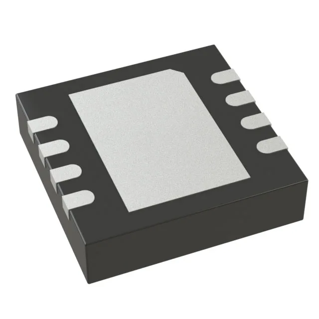
Analog Devices LTC2641CDD-14#PBF — Microcontrollers & Processors (MCU / MPU / DSP)

LTC2641CDD-14#PBF 14-Bit R-2R DAC, SPI, 8-DFN

MPNLTC2641CDD-14#PBF
End of Life

Analog Devices LTC2641CDD-14#PBF, 14-bit voltage-output DAC, R-2R architecture, SPI interface, 8-WFDFN exposed pad package, tube.

$13.68Ref. price · indicative, final on quote
Packaging8-WFDFN Exposed Pad
StockContact for availability
Lead timeIn Stock wk
MOQ1 pcs
  • 100% new & originalTraceable channels only — no refurbs, no pulls, no remarked parts.
  • Date & lot codes on quoteStated per line before you commit; label photos on request.
  • MSL-compliant ESD packingMoisture-sealed bags with indicator cards; reels photo-verified.
  • PayPal buyer protectionPay by T/T, PayPal or Payoneer — card payments covered end to end.

Specifications

LTC2641CDD-14#PBF Technical Specifications
ParameterValue
Output typeVoltage - Unbuffered
Mounting typeSurface Mount
Reference typeExternal
Voltage - supply, analog2.7V ~ 5.5V
Voltage - supply, digital2.7V ~ 5.5V
InterfaceSPI
Operating temperature0°C ~ 70°C
PackageTube
ArchitectureR-2R
INL (DNL)±0.5, ±0.5
Settling time1µs (Typ)
Number of bits14
Case8-WFDFN Exposed Pad
Differential outputNo
Number of d (A converters)1

Product details

14-bit R-2R DAC with 1 µs settling

The LTC2641CDD-14#PBF is a single-channel, 14-bit voltage-output DAC built on an R-2R ladder architecture. The R-2R topology is inherently monotonic and produces low glitch energy, so no external deglitching filter is needed in most signal-chain designs. Settling time is 1 µs typical to ±0.5 LSB — fast enough for closed-loop control loops updating at hundreds of kilohertz. The SPI data interface accepts clock rates up to 50 MHz, keeping the serial transaction time well under the settling window. INL and DNL are both ±0.5 LSB maximum, guaranteeing monotonicity and no missing codes across the full 14-bit transfer curve.

Single-supply rail and board fit

The output is voltage-unbuffered, meaning the DAC output impedance is the R-2R ladder's own (typically 5 kΩ to 10 kΩ). A downstream op-amp buffer is expected when driving loads below 10 kΩ or when the output must drive a long trace. The reference input is external — the full-scale output equals the reference voltage times the DAC gain (1× for this part). Packaged in an 8-lead WFDFN with exposed pad (3×3 mm body — supplier device package 8-DFN). Tube shipment — 100 pieces per tube.

Active lifecycle and compliance

RoHS3 compliant (2015/863/EU) with no exemptions. The lead finish on the DFN package is matte tin over nickel barrier — no SnPb or other restricted substances.

Frequently asked questions

What is the closest functional second-source to the LTC2641CDD-14#PBF?

The AD5541ARZ from Analog Devices is a close functional match — same R-2R architecture, same SPI interface, same ±0.5 LSB INL/DNL spec, and same voltage-unbuffered output. The key difference is resolution: the AD5541ARZ is 16-bit, two bits higher than the 14-bit LTC2641CDD-14#PBF. Package is also an 8-lead SOIC (vs 8-DFN), so a board layout change is required.

Can the LTC2641CDD-14#PBF drop into a board designed for the AD5541ARZ?

No — the packages differ. The LTC2641CDD-14#PBF uses an 8-DFN (3×3 mm) with exposed pad, while the AD5541ARZ is an 8-lead SOIC. The pin functions are similar (SPI, reference, output, supply), but the footprint, thermal pad, and pin spacing are not compatible. A board spin or adapter is required.