Quad 12-bit DAC with SPI — what the ratings mean for your BOM
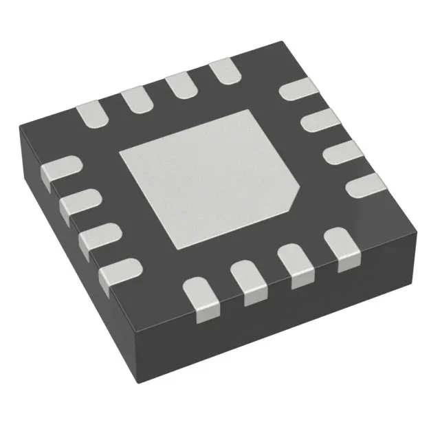
The LTC2634CUD-HZ12#PBF is a quad 12-bit digital-to-analog converter from Analog Devices, packaged in a 16-QFN 3x3 mm footprint. It delivers four independent voltage-buffered outputs via a single SPI bus — one chip handles four analog setpoints, saving board space over four separate single-channel DACs. The 12-bit resolution with ±1 LSB max INL/DNL means the output voltage lands within 1/4096 of full scale from the ideal value. For a 5V reference, that is about 1.2 mV of absolute accuracy — tight enough for most trim, bias, and setpoint loops without external calibration. Settling time is 4.8 µs typical to within 1 LSB. That sets the per-channel update rate ceiling around 200 kHz — fast enough for audio-rate control loops or waveform generation, but not for high-speed arbitrary waveform synthesis.
Supply rails and reference — single 5V operation
Both analog and digital supply rails are 5V — no separate DVCC or split-rail requirement. This simplifies the power tree: a single 5V rail feeds the DAC and the MCU's SPI port, with the analog output swing rail-to-rail from 0V to 5V. The reference can be either external (applied to the REF pin) or internal — the part integrates a 10 ppm/°C typical reference. Using the internal reference saves one external component and one PCB trace; using an external reference lets you match the DAC span to an existing system reference voltage.
Package and board-fit — 16-QFN with exposed pad
Tube packaging means the parts ship in anti-static tubes, not tape-and-reel. For a kitting line feeding a pick-and-place, plan to transfer to a feeder-compatible carrier or hand-place for prototype runs — the tube format is common for engineering samples and low-volume production.
Temperature grade and lifecycle — commercial range, active production
This covers most bench, lab, and indoor industrial equipment but not extended-temperature environments like engine bays or outdoor telecom cabinets.