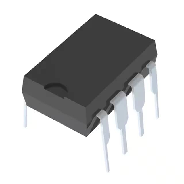
Analog Devices LTC1050CN8#PBF — Memory (DRAM / SRAM / Flash / EEPROM)

LTC1050CN8#PBF Zero-Drift Op-Amp, 2.5 MHz GBW, 0.5 µV Offset

MPNLTC1050CN8#PBF
End of Life

Linear Technology LTC1050CN8#PBF, Zero-Drift Amplifier, 1 Circuit, 8-DIP Package, Slew Rate 4V/µs, Gain Bandwidth 2.5 MHz, Supply 4.75 V to 16 V, Tube.

$7.27Ref. price · indicative, final on quote
Packaging8-DIP (0.300", 7.62mm)
StockContact for availability
MOQ1 pcs
  • 100% new & originalTraceable channels only — no refurbs, no pulls, no remarked parts.
  • Date & lot codes on quoteStated per line before you commit; label photos on request.
  • MSL-compliant ESD packingMoisture-sealed bags with indicator cards; reels photo-verified.
  • PayPal buyer protectionPay by T/T, PayPal or Payoneer — card payments covered end to end.

Specifications

LTC1050CN8#PBF Technical Specifications
ParameterValue
Mounting typeThrough Hole
Amplifier typeZero-Drift
Voltage - input offset0.5 µV
Voltage - supply span4.75 V
Current - supply1mA
Current - input bias10 pA
Operating temperature-40°C ~ 85°C
Gain bandwidth product2.5 MHz
PackageTube
Slew rate4V/µs
Case8-DIP (0.300\", 7.62mm)
Number of circuits1

Product details

Precision zero-drift amplifier in a through-hole package

The LTC1050CN8#PBF is a single zero-drift operational amplifier from Linear Technology, designed for applications that demand extremely low input offset voltage and minimal drift over temperature and time. With a typical offset of 0.5 µV and input bias current of 10 pA, this part is suited for precision DC measurement, thermocouple amplifiers, and medical instrumentation front-ends where accuracy cannot be traded off. The 2.5 MHz gain-bandwidth product and 4 V/µs slew rate provide enough bandwidth for low-frequency signal conditioning without sacrificing stability. Housed in an 8-DIP (0.300", 7.62 mm) through-hole package, it fits socketed or breadboard prototypes as well as production boards that favor hand-solderable DIP footprints. The supply range of 4.75 V to 16 V covers single-supply and split-supply rails common in industrial and lab equipment. Operating temperature from -40°C to 85°C covers industrial environments.

Zero-drift topology — what it means for your signal chain

The zero-drift architecture continuously auto-corrects the input offset, so the 0.5 µV typical offset stays flat across the temperature range and over years of operation. That matters for circuits like load-cell readouts, precision current shunts, or DAC output buffers where a few microvolts of drift would shift the system accuracy out of spec. The 10 pA input bias current also suits high-impedance sources — pH probes, photodiode preamps, or high-value resistive dividers — without needing a second buffer stage. The 1 mA supply current per amplifier keeps the thermal budget modest in multi-channel panels.

Slew rate and bandwidth — matching the signal

Gain-bandwidth product is 2.5 MHz and slew rate is 4 V/µs.

Frequently asked questions

What are the alternatives to LTC1050CN8#PBF?

The AD8628ARZ and AD8638ARZ are zero-drift amplifiers from ADI with similar offset and bias specs, but they come in surface-mount packages (SOIC) and offer rail-to-rail output. They are not pin-compatible drop-ins for the 8-DIP LTC1050CN8#PBF. The AD629ANZ is a different amplifier type (current sense) and not a zero-drift substitute.

What is the pinout of LTC1050CN8#PBF?

The LTC1050CN8#PBF uses the standard 8-DIP pinout for single op-amps: pin 1 (offset null), pin 2 (inverting input), pin 3 (non-inverting input), pin 4 (V-), pin 5 (offset null), pin 6 (output), pin 7 (V+), pin 8 (NC). Refer to the LTC1050 datasheet for the exact pin diagram.