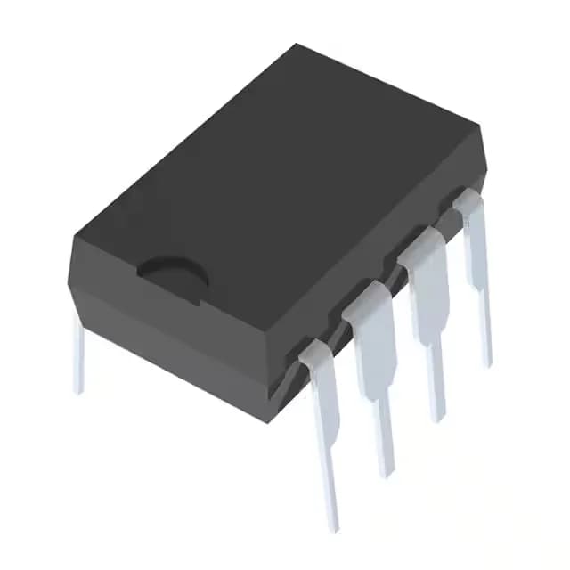
Analog Devices LTC1047CN8#PBF — Memory (DRAM / SRAM / Flash / EEPROM)

LTC1047CN8#PBF Zero-Drift Op-Amp, 200 kHz, 0.2V/µs, 8-DIP

MPNLTC1047CN8#PBF
End of Life

Analog Devices LTC1047CN8#PBF, Chopper (Zero-Drift) dual op-amp, 200 kHz GBW, 0.2V/µs slew rate, 3 µV offset, 80 µA supply, 4.75-16V, 8-DIP (0.300", 7.62mm), Through Hole, Tube, 0°C to 70°C, ROHS3 compliant, Active.

$13.29Ref. price · indicative, final on quote
Packaging8-DIP (0.300", 7.62mm)
StockContact for availability
MOQ1 pcs
  • 100% new & originalTraceable channels only — no refurbs, no pulls, no remarked parts.
  • Date & lot codes on quoteStated per line before you commit; label photos on request.
  • MSL-compliant ESD packingMoisture-sealed bags with indicator cards; reels photo-verified.
  • PayPal buyer protectionPay by T/T, PayPal or Payoneer — card payments covered end to end.

Specifications

LTC1047CN8#PBF Technical Specifications
ParameterValue
Mounting typeThrough Hole
Amplifier typeChopper (Zero-Drift)
Voltage - input offset3 µV
Voltage - supply span4.75 V
Current - supply80µA (x2 Channels)
Current - input bias5 pA
Operating temperature0°C ~ 70°C
Gain bandwidth product200 kHz
PackageTube
Slew rate0.2V/µs
Case8-DIP (0.300\", 7.62mm)
Number of circuits2

Product details

Chopper-stabilized precision for low-level DC signals

The LTC1047CN8#PBF is a dual-channel chopper (zero-drift) operational amplifier from Analog Devices. Its internal auto-zero architecture holds input offset voltage to 3 µV. The 200 kHz gain-bandwidth product and 0.2 V/µs slew rate indicate DC-optimised performance.

Package and sourcing reality

The 8-DIP (0.300", 7.62 mm) through-hole package suits prototyping and wave-solder assembly. The supplier device package is 8-PDIP, and the part ships in a tube. Lifecycle status is Active with ROHS3 compliance.

Second-source and cross-shop context

The closest functional peer in the same commercial temperature band and through-hole footprint is the AD706JNZ, a general-purpose dual op-amp with 800 kHz GBW and 0.15 V/µs slew rate but a 30 µV offset — an order of magnitude higher than the LTC1047CN8#PBF. For a design that cannot tolerate that offset drift, the LTC1047CN8#PBF is the correct choice. The AD827JNZ and AD712KNZ are faster parts (50 MHz and 4 MHz respectively) with 300 µV offset, suited to different application tiers entirely.

Frequently asked questions

Does LTC1047CN8#PBF require a heat sink?

No. The total supply current for both channels is 80 µA, which keeps self-heating negligible at any rated supply voltage within the 0°C to 70°C operating range. No heatsink is needed.

What is the closest functional second-source to LTC1047CN8#PBF?

The AD706JNZ is a through-hole dual op-amp in the same temperature grade, but its 30 µV offset is ten times higher than the LTC1047CN8#PBF's 3 µV. For designs that can tolerate that drift, the AD706JNZ is a pin-compatible alternate; for precision DC applications, the LTC1047CN8#PBF remains the correct part.