Active production — still a design-in candidate
The LT8609SEV#PBF: ROHS3 compliant per the manufacturer, with no REACH or halogen-free restriction flagged in the listing — the bill-of-materials compliance check is straightforward.
Input range and output capability
Operates from a 3 V minimum input up to 42 V maximum, covering 12 V and 24 V industrial rails as well as 48 V telecom buses with margin. The 2 A continuous output is rated for moderate loads — sensor nodes, auxiliary supplies, or post-regulation stages. The adjustable output voltage floor is 0.782 V, allowing generation of sub-1 V rails for low-voltage digital cores, while the maximum output matches the input rail (up to 42 V). Switching frequency is programmable from 200 kHz to 2.2 MHz via the RT pin or SYNC input — a higher frequency shrinks the inductor footprint at the cost of switching losses; a lower frequency improves efficiency at light loads.
Thermal and package constraints
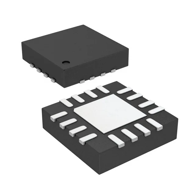
Housed in a 16-lead 3 mm × 3 mm LQFN with exposed pad (16-LQFN). The small footprint demands careful thermal vias under the pad to the ground plane — the junction-to-ambient thermal resistance depends heavily on the PCB copper area, not just the package itself. Rated for -40°C to +125°C junction temperature, which covers industrial and automotive under-hood environments. The 2 A output at high ambient requires derating; the datasheet's thermal derating curve (not reproduced here) governs the actual current limit in a given layout.
Synchronous rectification and efficiency
Built-in synchronous rectifier eliminates the external freewheeling diode, improving efficiency at high switching frequencies and reducing the BOM count. The internal top and bottom FETs are sized for the 2 A rating; no external catch diode is needed.