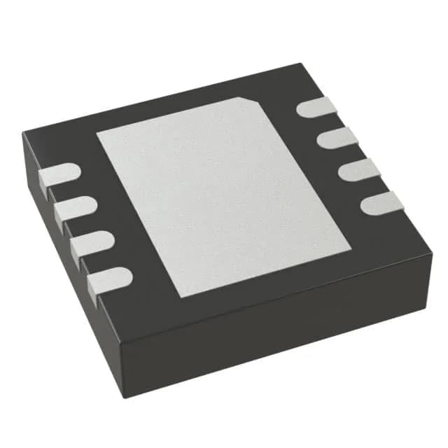
Analog Devices LT6234IDD#TRPBF — Logic ICs

LT6234IDD#TRPBF dual op-amp, 60 MHz, 17 V/µs

MPNLT6234IDD#TRPBF
End of Life

Analog Devices LT® series LT6234IDD#TRPBF, dual general-purpose op-amp, 60 MHz gain bandwidth, 17 V/µs slew rate, rail-to-rail output, 8-WFDFN exposed pad, -40°C to 85°C.

$8.93Ref. price · indicative, final on quote
Packaging8-WFDFN Exposed Pad
StockContact for availability
MOQ1 pcs
  • 100% new & originalTraceable channels only — no refurbs, no pulls, no remarked parts.
  • Date & lot codes on quoteStated per line before you commit; label photos on request.
  • MSL-compliant ESD packingMoisture-sealed bags with indicator cards; reels photo-verified.
  • PayPal buyer protectionPay by T/T, PayPal or Payoneer — card payments covered end to end.

Specifications

LT6234IDD#TRPBF Technical Specifications
ParameterValue
SeriesLT®
Output typeRail-to-Rail
Mounting typeSurface Mount
Amplifier typeGeneral Purpose
Voltage - input offset75 µV
Voltage - supply span12.6 V
Current - supply1.05mA (x2 Channels)
Current - input bias1.5 µA
Current - output (Channel)55 mA
Operating temperature-40°C ~ 85°C
Gain bandwidth product60 MHz
PackageTape & Reel (TR); Cut Tape (CT)
Slew rate17V/µs
Case8-WFDFN Exposed Pad
Number of circuits2

Product details

60 MHz dual op-amp in a 3x3 DFN — signal-chain fit

It delivers rail-to-rail output swing across a supply span from 3 V to 12.6 V, drawing 1.05 mA per channel.

75 µV offset and 55 mA output — DC precision and drive

Input offset voltage is specified at 75 µV, giving the LT6234IDD#TRPBF enough DC accuracy for 12-bit signal paths without external nulling. The 1.5 µA input bias current is bipolar-typical and matters when the source impedance exceeds a few kilohms — plan for a bias-current error term in the noise gain calculation.

The exposed-pad DFN package is MSL 1 per the LT® family typical — verify the specific MSL rating on the reel label before skipping a bake step.

8-DFN footprint — thermal and layout notes

The pad is electrically connected to the negative supply (V−) on this device, so the PCB copper pour must be at the same potential. Solder-paste coverage on the pad should be about 50% stencil aperture to avoid floating the part during reflow.

Frequently asked questions

What is the closest functional second-source for LT6234IDD#TRPBF?

The ADA4841-2YRMZ-R7 is a parametric peer: a dual rail-to-rail output op-amp with 80 MHz gain-bandwidth, 13 V/µs slew rate, and 40 µV typical offset. Footprints differ (8-DFN vs 8-MSOP), so a PCB respin is required to qualify the alternate.