Analog Devices LT6231CDD#TRPBF — Logic ICs

LT6231CDD#TRPBF Dual Rail-to-Rail Op-Amp, 215 MHz GBW

MPNLT6231CDD#TRPBF
End of Life

Analog Devices LT® series LT6231CDD#TRPBF, dual general-purpose op-amp, 215 MHz GBW, 70V/µs slew rate, rail-to-rail output, 3V to 12.6V supply, 8-WFDFN exposed pad package, 0°C to 70°C.

$6.97Ref. price · indicative, final on quote
Packaging8-WFDFN Exposed Pad
StockContact for availability
MOQ1 pcs
  • 100% new & originalTraceable channels only — no refurbs, no pulls, no remarked parts.
  • Date & lot codes on quoteStated per line before you commit; label photos on request.
  • MSL-compliant ESD packingMoisture-sealed bags with indicator cards; reels photo-verified.
  • PayPal buyer protectionPay by T/T, PayPal or Payoneer — card payments covered end to end.

Specifications

LT6231CDD#TRPBF Technical Specifications
ParameterValue
SeriesLT®
Output typeRail-to-Rail
Mounting typeSurface Mount
Amplifier typeGeneral Purpose
Voltage - input offset450 µV
Voltage - supply span12.6 V
Current - supply3.3mA (x2 Channels)
Current - input bias5 µA
Current - output (Channel)30 mA
Operating temperature0°C ~ 70°C
Gain bandwidth product215 MHz
PackageTape & Reel (TR); Cut Tape (CT)
Slew rate70V/µs
Case8-WFDFN Exposed Pad
Number of circuits2

Product details

Package and mounting

It runs rail-to-rail on the output side, which matters when you are swinging close to the supply rails in a single-supply signal chain. The 3.3 mA per-channel supply current is the price you pay for that speed — this is not a micropower part, it is a signal-conditioning amp for ADC drivers, video buffers, or high-speed filter stages where bandwidth and settling time drive the choice.

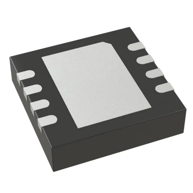
Package and rework — the 8-DFN exposed pad

The 8-WFDFN exposed pad package (3x3 mm body) is a QFN-style part with a center thermal pad. That pad needs a via stitch to the ground plane to pull heat out of the die — without it the junction climbs fast if you push the 30 mA per-channel output near the supply rails. Rework is doable with hot air if you preheat the board to 100°C and use a fine-tip nozzle; the exposed pad gives you a visual alignment check when the part self-centers during reflow.

Temperature grade and deployment boundary

Fine for bench instruments, office equipment, audio gear, or indoor telecom — but do not spec it into a motor drive enclosure, engine bay, or outdoor cabinet without a temperature chamber test. The 450 µV input offset voltage is typical for a high-speed bipolar input stage; if you need sub-100 µV offset for precision DC, look at a chopper-stabilized amp instead.

Frequently asked questions

What is a functional equivalent or second-source for LT6231CDD#TRPBF?

The AD8028 has a higher slew rate (100 V/µs) and lower input offset voltage (200 µV), but comes in an MSOP-8 package rather than the DFN. Check the pinout and footprint before substituting — the packages are not drop-in compatible.