100 MHz GBP, 25 V/µs — the signal-chain workhorse
It delivers rail-to-rail output swing while drawing 2.8 mA per channel from a supply spanning 2.5 V to 12.6 V.
The 2.5 V to 12.6 V supply span covers common rails: single 3.3 V, 5 V, or split ±5 V. At 5 V single supply, the rail-to-rail output stage swings within millivolts of both rails, so a 0 V to 5 V ADC input range is usable without level shifting. Each channel can source or sink 40 mA, enough to drive a 50 Ω back-terminated line or a moderate SAR ADC input. The input bias current is 3.8 µA — not a precision amp, but fine for circuits where source impedance stays below a few kΩ.
Package and thermal — the exposed-paddle reality
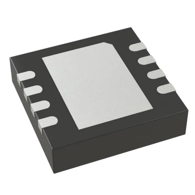
The 8-WFDFN with exposed pad (8-DFN 3x3 mm) needs the thermal pad soldered to a PCB copper plane to keep junction temperature in check. Without that thermal via stitch, the 40 mA per channel output current at elevated ambient can push the die past the 85°C operating limit. No heatsink is required — the PCB copper does the job — but the datasheet pad layout must be followed. MSL 1 out of the bag, so no bake before reflow unless the seal is compromised.