350 kHz GBW, 20 µV offset — the precision trade-off
The LT6010AIDD#PBF: The 20 µV typical input offset voltage means DC errors stay low enough to skip a trim pot in many sensor-conditioning paths — but the 2 nA input bias current is the figure to watch when the source impedance climbs above 100 kΩ. Rail-to-rail output swing at 20 mA per channel lets it drive a 2.5 V reference into a 125 Ω load without losing headroom. Supply range from 2.7 V to 36 V covers single 3.3 V rails up to ±15 V bipolar supplies — no secondary regulator needed for the op amp rail in a mixed-voltage design.
8-DFN package and thermal path
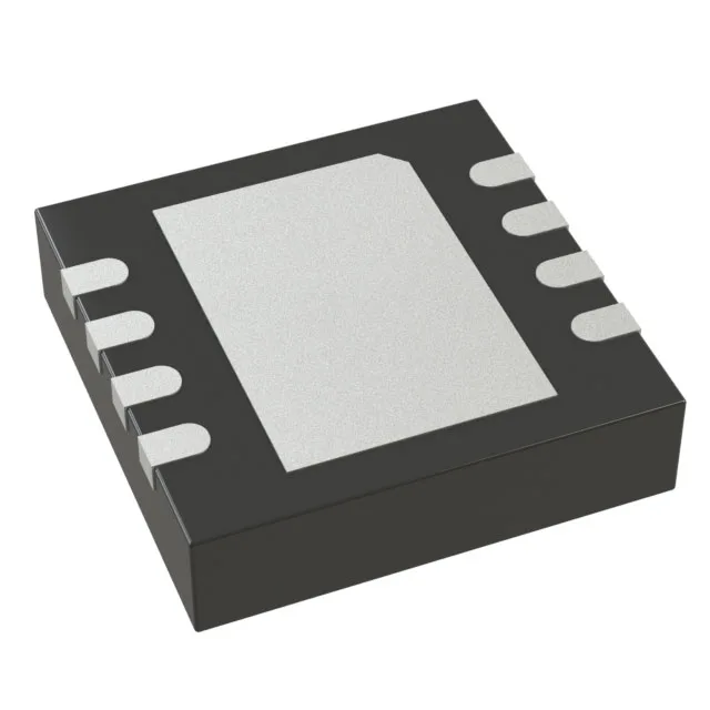
Housed in an 8-WFDFN with exposed pad (3×3 mm body), the LT6010AIDD#PBF relies on the pad soldered to a PCB copper plane for thermal dissipation. Surface-mount assembly with the exposed pad means the solder paste stencil aperture for the pad should match the datasheet-recommended footprint — the pad is the primary thermal and electrical ground connection.