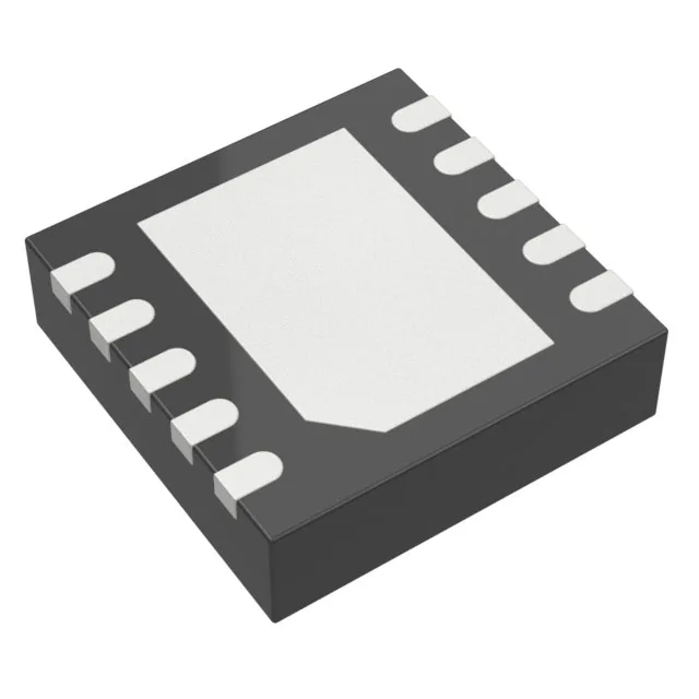
Package and board-fit — 10-DFN with exposed pad
The LT3463EDD#PBF comes in a 10-WFDFN exposed-pad package (3×3 mm body, supplier device package 10-DFN). The exposed paddle on the underside must be soldered to a copper land on the PCB — this is the primary thermal path for the 180 mA and 320 mA switch currents, and it also provides a low-impedance ground return.
Dual-rail output — positive and negative from a single IC
This is a dual-output step-up regulator that generates both a positive and a negative rail from a single input. The topology combines a boost converter for the positive output and a charge pump for the negative rail, so you get ±1.25 V to ±40 V adjustable outputs without needing a separate inverting stage. The two switch pins are rated 180 mA (one switch) and 320 mA (the other switch) — the higher-current side typically drives the boost, the lower-current side the charge pump.
Temperature grade and environment
The part is intended for indoor, temperature-controlled equipment (test gear, bench supplies, base-station line cards) rather than automotive or industrial outdoor enclosures. If your BOM calls for -40 °C operation, the LT3463EDD#PBF is not the fit; look at the ADP5070AREZ peer which carries the wider industrial temperature range.
Lifecycle and compliance — active, RoHS3, no obsolescence risk
The RoHS3 status means it meets the latest EU restriction exemption rules — no need to manage a transition exemption expiry on your BOM.