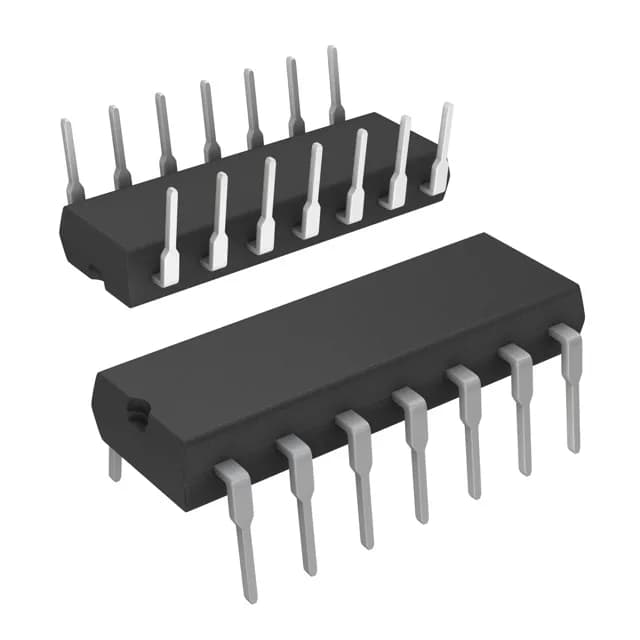
The LT1058CN#PBF is a quad JFET-input operational amplifier from the Analog Devices LT® series, packaged in a 14-lead PDIP (0.300-inch, 7.62 mm body) for through-hole assembly. Input bias current is 7 pA, and input offset voltage is 250 µV — figures that suit precision analog signal conditioning in industrial control, audio processing, data acquisition front-ends, and test equipment where through-hole prototyping or high-reliability socketed designs are preferred.
5 MHz GBP and 13 V/µs slew — what the speed ratings mean
With a 5 MHz gain-bandwidth product and 13 V/µs slew rate, the LT1058CN#PBF sits in the medium-speed tier of JFET op-amps. The 5 MHz GBP supports closed-loop gains up to about 10 at 500 kHz before open-loop roll-off limits accuracy; the 13 V/µs slew rate allows full-power output swings up to roughly 100 kHz at 20 V peak-to-peak. For audio applications, this covers the full audible band with margin. For data acquisition, the settling time to 0.01% will be in the low-microsecond range — adequate for multiplexed ADC drivers sampling below 100 kSPS. If your signal chain needs faster edges (e.g., driving a high-speed ADC input), the AD713 family (20 V/µs) offers a higher slew rate, though in a surface-mount SOIC package.
Input precision — 7 pA bias, 250 µV offset
The 7 pA input bias current is typical for JFET-input amplifiers and allows the LT1058CN#PBF to interface with high-impedance sources (e.g., photodiodes, piezoelectric sensors, pH probes) without significant voltage error from bias current flowing through source resistance. The 250 µV input offset voltage sets the DC accuracy floor: for a gain of 100, the output offset contributed by the amplifier alone is 25 mV. If your error budget demands lower offset, the AD712 family specifies 300 µV (dual) but with a lower 4 MHz GBP — a trade-off between DC precision and bandwidth.
Active lifecycle and RoHS compliance — no LTB concern
The #PBF suffix confirms a lead-free (RoHS) finish — compatible with lead-free reflow profiles for through-hole wave soldering, though the through-hole package is typically hand-soldered or wave-soldered.