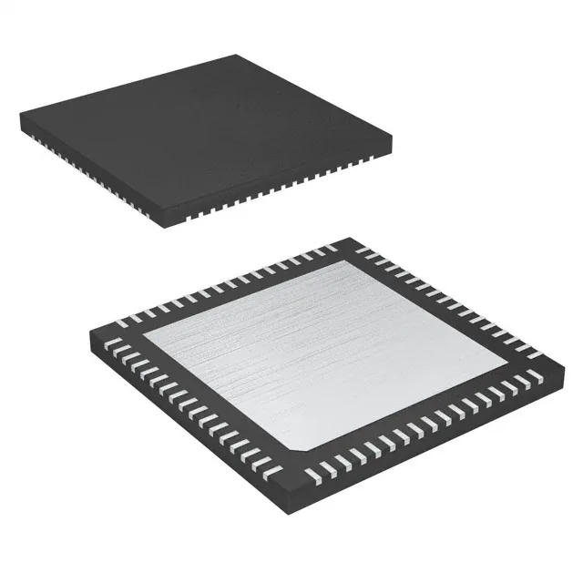
Jitter attenuator with 14-output fanout for RF clock trees
The Analog Devices HMC7044LP10BE is a jitter attenuator with an integrated PLL, designed to clean up noisy reference clocks and distribute low-jitter timing to multiple destinations. It accepts CML, CMOS, LVDS, or LVPECL inputs and provides up to 14 differential outputs in CML, LVDS, or LVPECL formats, covering a maximum frequency of 3.2 GHz. The 4:14 input-to-output ratio lets a single device replace several clock buffers and PLLs in a high-speed converter or RF signal chain.
3.2 GHz ceiling and 14 outputs — sizing the clock tree
The 3.2 GHz maximum frequency covers L-band and lower C-band local-oscillator distribution, as well as high-speed ADC/DAC sample clocks up to several giga-samples per second. With 14 outputs from a single PLL, the HMC7044LP10BE can feed an entire multi-channel receiver or transmitter array without cascading multiple clock chips, saving board area and reducing additive jitter from extra stages. The supply range of 3.135 V to 3.465 V aligns with standard 3.3 V rails; the 68-LFCSP-VQ (10x10) exposed-pad package requires a solid thermal and ground connection through the center paddle for best phase-noise performance.
68-lead LFCSP — footprint and thermal considerations
The 68-VFQFN exposed-pad package (LFCSP-VQ, 10x10 mm) is a surface-mount, leadless design with a large center paddle.