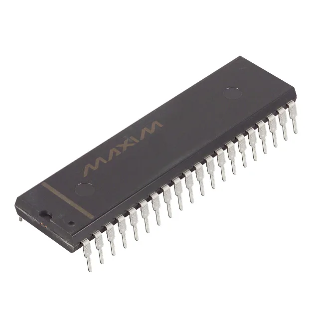
Active 8051 MCU for legacy and new designs
The DS80C320-MCG+: With 256 x 8 bytes of on-chip RAM and no internal program memory (ROMless), this part relies on external memory for code storage — a common architecture for designs that need flexible memory sizing or in-system reprogramming.
What the 25 MHz clock and ROMless design mean for your BOM
The 25 MHz clock rate sets the instruction throughput ceiling for this 8051 derivative — each machine cycle takes 4 clock periods, so the effective instruction rate is about 6.25 MIPS, enough for control-oriented tasks like industrial I/O handling or serial protocol bridging. Because the part is ROMless, you must budget for an external parallel flash or EPROM plus an address latch (typically a 74HC373) to hold the program image, adding 2-3 ICs and board area beyond the MCU itself. The 40-pin DIP package (0.600-inch row spacing) is a through-hole footprint — it suits prototyping boards, socketed production, or rework scenarios where a soldered QFP would be harder to replace.
Peripheral set and voltage requirements
On-chip peripherals include a power-fail reset and a watchdog timer (WDT), which together can supervise supply brownouts and code hangs without an external supervisor IC — a cost saving in high-volume embedded control. Connectivity covers EBI/EMI for external memory access, plus SIO and a UART/USART for serial communication with sensors, displays, or host controllers.
The 32 general-purpose I/O pins, combined with the external memory interface, give enough headroom for a small keypad-and-LCD panel or a handful of relay drivers and sensor inputs.
Sourcing and compliance
RoHS3 compliant (2011/65/EU + 2015/863), with no lead, mercury, cadmium, or other restricted substances above threshold levels in the homogeneous material.