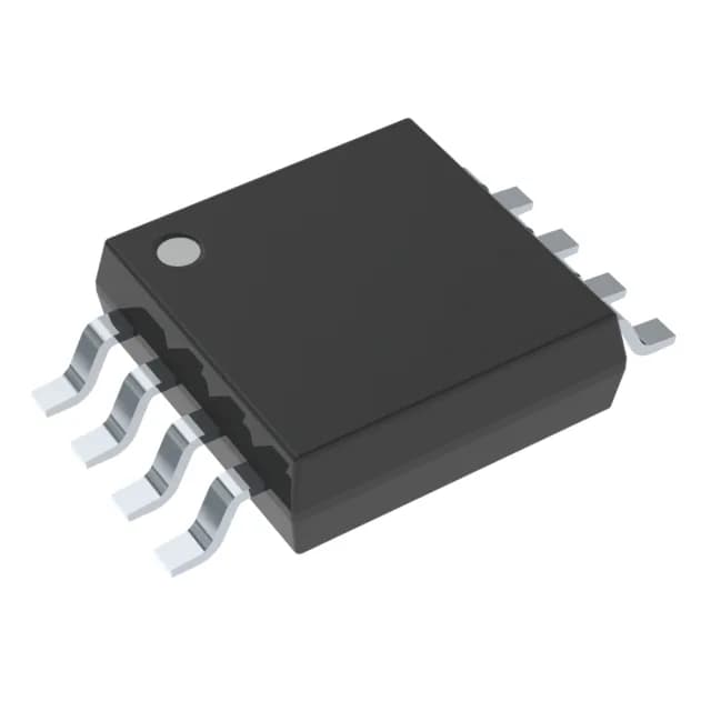
100 taps, 100 kΩ, linear — the trim pot for production calibration
The Maxim Integrated DS1804U-100+T&R is a single-channel, non-volatile digital potentiometer with 100 tap positions and a linear taper over a 100 kΩ end-to-end resistance. It stores the wiper setting in non-volatile memory, so the calibration holds through a power cycle without a microcontroller intervention or external EEPROM. The three-wire Up/Down interface (U/D, INC, CS) is straightforward for a firmware engineer to drive from any GPIO bank — no SPI or I²C bus required, which saves pins on a small MCU. The 2.7 V to 5.5 V supply range covers 3.3 V and 5 V logic rails commonly found in industrial sensor transmitters, programmable power supplies, and audio gain stages.
Wiper resistance and temperature drift — the hidden limits
The wiper resistance is 400 Ω typical, which adds a fixed series offset at the wiper terminal. In a voltage-divider configuration that offset is negligible, but in rheostat mode (wiper to one end) the minimum resistance is 400 Ω, not zero — a detail that matters when setting a low-impedance bias point. The temperature coefficient is 750 ppm/°C typical, so a 100 kΩ setting drifts about 75 Ω per degree. For a room-temperature trim that is fine; for a -40°C to 85°C span the drift can shift the set point by several percent, so budget the tolerance (±20%) plus the tempco in the system error analysis.
Active production, RoHS3, and the 8-uMAX footprint
The DS1804U-100+T&R carries an Active product status and is ROHS3 compliant. The 8-uMAX/uSOP package (3.00 mm width, 0.118" pitch) is a common footprint shared with the DS1804-050 and other 8-pin digital pots from Maxim, so a board layout can accommodate multiple resistance values on the same pad pattern. Cut Tape (CT) is also available for prototype quantities.
Sourcing and BOM fit
This part is sourced through independent distribution and quoted to order against an RFQ. The DS1804U-050 variant offers 50 kΩ end-to-end resistance with the same tap count and interface, useful when a lower impedance range is needed without changing the PCB layout.