70 ns access time and the byte-wide bus
The DS1249AB-70# is a 2 Mbit NVSRAM organized as 256K x 8 bits, accessed over a parallel byte-wide bus with a 70 ns access time. That 70 ns figure sets the read-cycle floor for the host controller — a 8-bit MCU or FPGA reading at 70 ns intervals sees a theoretical 14.3 MHz bus rate, though the actual throughput is lower once the address setup, hold, and data latch times are factored in. The memory cell combines SRAM speed with on-chip non-volatile storage — no external battery or EEPROM is needed to retain data across power cycles. The write cycle time matches the read access at 70 ns for word and page operations.
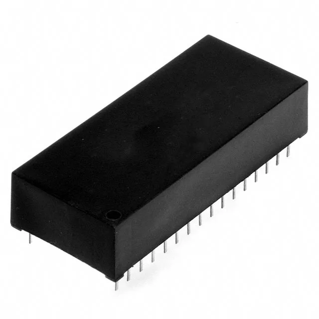
Housed in a 32-pin DIP module (0.600" body width) with an EDIP (encapsulated DIP) package. The through-hole footprint mates with standard 0.600" DIP sockets or can be soldered directly into a plated-through-hole PCB. The EDIP construction encapsulates the NVSRAM die and the non-volatile storage element in a single module — no separate lithium cell or capacitor is present.
Lifecycle and compliance posture
Supplied in Tube packaging — the standard through-hole DIP format.