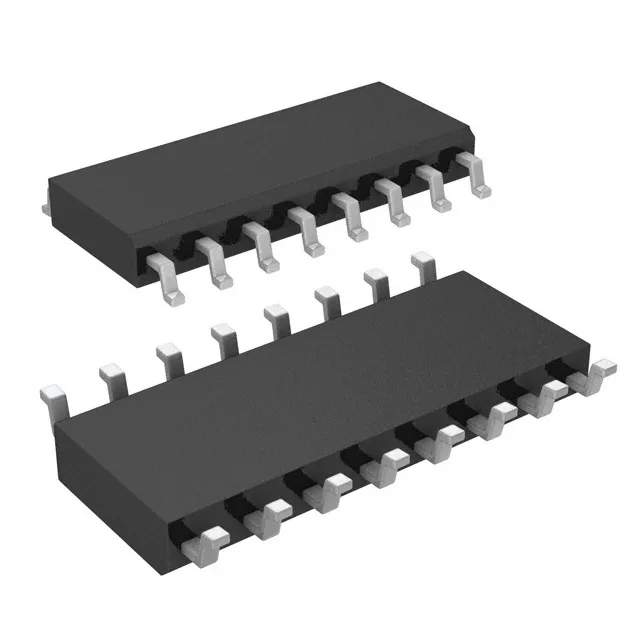
Supply flexibility drives the fit
The DG413CY+T: The 45 Ohm max on-resistance is flat enough across the signal range for 12-bit acquisition; the 3 Ohm max channel-to-channel matching keeps the gain error between paths below 0.01 % in a unity-gain buffer configuration.
Signal integrity specs that matter in a multiplexed path
Charge injection is 5 pC typical — that is the charge dumped onto the signal node when the switch opens. Into a 10 pF hold capacitor on a sample-and-hold front end, it produces a 500 mV glitch; you budget that into the acquisition settling time. Off-leakage maxes at 250 pA, so a 10 kOhm source impedance sees less than 2.5 µV of voltage error from leakage alone. Crosstalk is -85 dB at 1 MHz — a -85 dB figure means a 1 Vpp signal on one channel couples less than 60 µV into an adjacent off channel. That is clean enough for a 16-bit system where the LSB at a 5 V reference is 76 µV. Channel capacitance is 9 pF on both the source and drain sides, which sets the -3 dB bandwidth to roughly 390 MHz into a 50 Ohm load — well above the audio or low-frequency multiplexing bands this part is designed for. Switching times are 175 ns on, 145 ns off — the part toggles at about 3 MHz in a break-before-make sequence. That is fast enough to scan 16 channels in under 3 µs with settling, which suits a data-acquisition system sampling at 100 kSPS per channel.