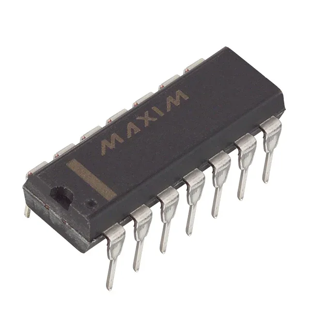
Dual SPDT switch in a 14-DIP through-hole package
The DG307ACJ+ is a dual SPDT analog switch from Analog Devices, packaged in a 14-DIP (0.300", 7.62mm) through-hole package. Each of the two independent switches routes a common input to one of two outputs, implementing a 2:1 multiplexer/demultiplexer function per channel.
On-resistance and signal integrity floor
Maximum on-state resistance is 50 Ohms, setting the insertion loss floor for the signal path. In a 50-Ohm system, this adds a 6 dB attenuation when the switch is inserted between source and load; in a high-impedance path the voltage divider effect is negligible. Off-state leakage is 5 nA maximum, and channel capacitance to ground is 14 pF per pole. Together they determine the isolation at high frequencies — at 1 MHz the 14 pF capacitance presents roughly 11 kOhm of parasitic coupling, so the off-isolation degrades above a few hundred kilohertz.
Switching speed and timing margin
Turn-on time is 250 ns maximum, turn-off 150 ns maximum. This 100 ns asymmetry means the break-before-make interval is at least 100 ns — the switch opens before the next channel closes, preventing momentary short circuits between signal sources in multiplexed applications. Charge injection is 12 pC typical. In a sample-and-hold front end driving a 10 nF hold capacitor, this injects 1.2 mV of offset error; for precision acquisition below 12 bits the charge-injection pedestal must be cancelled or calibrated out.
Crosstalk isolation and dual-supply range
Crosstalk between channels is -74 dB at 500 kHz. For a 10 Vpp signal on one channel, the coupled feedthrough on the adjacent channel is roughly 2 mVpp — adequate for 10-bit separation but marginal for 16-bit multiplexed data acquisition at that frequency. Dual-supply range is ±5 V to ±18 V. The analog signal swing tracks the supply rails minus the on-resistance drop; with ±15 V rails the switch handles ±13.5 Vpp cleanly before the internal FETs enter the linear region. Single-supply operation is not specified — the part is designed for bipolar rails.
This covers benchtop instrumentation, audio routing, and indoor telecom equipment but not automotive cabin or outdoor enclosures without climate control.