Switching speed and charge injection
The DG202CJ+: Maximum turn-on time is 600 ns and turn-off is 450 ns, which sets the throughput ceiling for multiplexing analog signals in a sampled-data system — the switch must settle before the downstream ADC samples. Charge injection is specified at 20 pC; this glitch couples onto the signal path when the switch transitions, so for high-impedance hold capacitors the injected charge can cause a voltage step that takes time to settle. Off-isolation is characterised by a crosstalk figure of -90 dB at 100 kHz, meaning less than 0.003% of a signal on one channel leaks onto an adjacent off channel at that frequency. Leakage current when off is 5 nA max, and each channel presents 5 pF of capacitance to ground in both the on and off states — these together determine the signal attenuation and bandwidth through the switch in a multiplexed front-end.
Through-hole DIP for prototyping and legacy boards
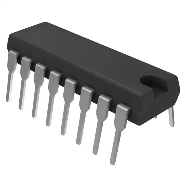
The 16-pin DIP package with 0.300-inch row spacing and 0.100-inch pin pitch is a standard through-hole footprint that fits breadboards, prototype boards, and existing PCB layouts that were designed around a DIP-16 analog switch.