Isolated gate driver with 4 A peak and 50 kV/µs CMTI
It delivers 4 A peak output current per channel, with 2500 Vrms isolation and a minimum common-mode transient immunity of 50 kV/µs. Propagation delay is 68 ns max, and rise/fall times are 12 ns typical.
50 kV/µs CMTI — the spec that keeps the gate drive clean
The 50 kV/µs common-mode transient immunity is the headline rating for this part. In a half-bridge or full-bridge topology, the high-side driver sees the switch node slam from ground to the DC bus voltage in tens of nanoseconds. If the isolator can't reject that edge, the output glitches, the power device turns on when it shouldn't, and the phase leg shoots through. 50 kV/µs covers most Si IGBT and SiC MOSFET switching edges up to 1200 V bus with reasonable layout margin.
4 A peak output — what it drives
4 A peak output lets this driver handle the gate charge of medium-power IGBTs (up to about 600 A / 1200 V class) and SiC MOSFETs in the 30–80 mΩ range. The 12 ns rise/fall time keeps switching losses in check. For larger modules, you'd step up to a 10 A or 20 A driver; for small FETs, this is overkill but works fine with a series gate resistor to tame the edge rate.
13-LGA package — rework considerations
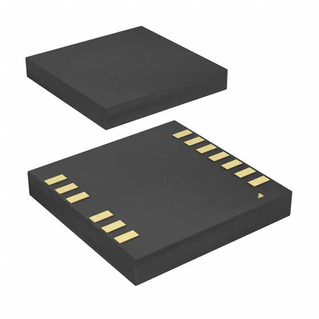
The 13-LGA (5x5 mm) package is a land-grid array with no leads. It's surface-mount and requires a solder-paste stencil and reflow profile, not a soldering iron.