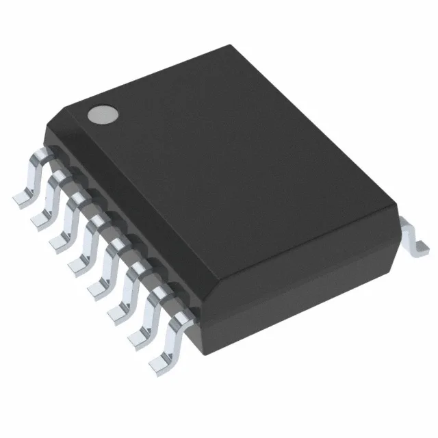
It uses magnetic coupling technology and is rated for 5000Vrms isolation — a figure that qualifies it for reinforced insulation in medical (IEC 60601) and industrial applications where galvanic isolation is a safety requirement. The two channels are configured with both inputs on side 1 (2/0 input-side/side-2 ratio), so this variant is for signals flowing in one direction only — from the primary-side supply domain to the isolated secondary side. Data rate is specified at 1Mbps maximum, with 100ns propagation delay and 40ns pulse-width distortion, which suits moderate-speed control signals, SPI-like interfaces up to 1 MHz, and general-purpose isolation of digital I/O lines. The supply range spans 3V to 5.5V on both sides, so it can interface directly with 3.3V or 5V logic without level translation.
IsoPower: what the integrated isolated supply means for the BOM
The key differentiator of the ADUM6200ARWZ versus a plain digital isolator is the integrated IsoPower DC-DC converter. Instead of routing a separate isolated 5V or 3.3V supply from a discrete transformer-and-rectifier stage, the part generates its own isolated output voltage from the input-side supply. This collapses a multi-component power-isolation stage into a single IC, saving board area and reducing procurement complexity. The trade-off is that the isolated power output is limited in current — the ADUM6200ARWZ is designed for the isolator's own secondary-side circuitry and light auxiliary loads, not for powering an entire isolated domain. For designs that need more secondary-side current, the ADuM620x family offers higher-drive variants.
CMTI and propagation delay — the margin-critical specs
Common-mode transient immunity is specified at a minimum of 25kV/µs. This is the part's ability to reject fast voltage transients between the input and output grounds — a critical parameter in motor-drive and inverter stages where IGBT or SiC switching edges can inject several kV/µs of common-mode noise across the isolation barrier. A CMTI below the transient slew rate will cause data corruption or output glitches. The 25kV/µs floor here is sufficient for most industrial drives operating at moderate switching frequencies; for SiC-based designs with edge rates exceeding 50kV/µs, a higher-CMTI isolator should be evaluated. Propagation delay is 100ns maximum in both directions, with a 40ns pulse-width distortion maximum. These numbers define the timing budget for the isolated path. At 1Mbps (1µs bit period), 100ns represents 10% of the bit time — acceptable for most control and status signals, but tight for high-speed synchronous interfaces where setup-and-hold margins are already constrained. The 2.5ns typical rise/fall time keeps the output edge clean and reduces the risk of signal-integrity issues on short traces.
Package and footprint — 16-SOIC wide-body
The wide-body SOIC provides the creepage distance needed to sustain the 5000Vrms isolation rating — the narrower SOIC-8 or SOIC-16 narrow-body packages cannot achieve this isolation level.