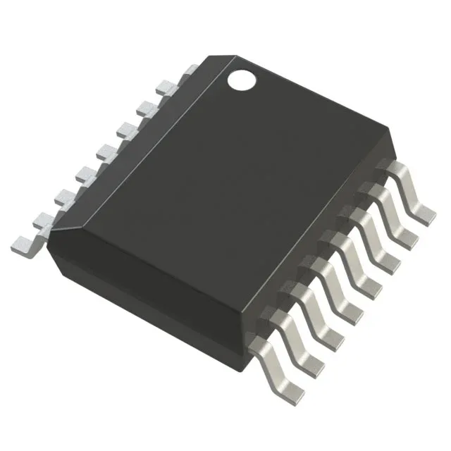
Four-channel magnetic isolator for mixed-voltage industrial buses
It delivers 150Mbps data rate across a 3000Vrms isolation barrier, with a 3/1 input-to-output channel split — three channels drive from Side 1 to Side 2, one channel runs reverse. Typical applications include isolated SPI/UART interfaces, industrial fieldbus isolation, motor-drive control signal isolation, and medical equipment where the 3000Vrms rating meets basic insulation requirements.
The 13ns max propagation delay (tpLH/tpHL) and 3ns max pulse-width distortion matter when you are sending gate-drive PWM or encoder signals across the barrier. With matched 13ns delays on both edges, the dead-time you program into the controller is what you actually get at the isolated side — no extra skew eating into your margin. If the CMTI is too low, the isolator can couple the transient onto the output and the controller sees a false edge. At 75kV/µs this part handles the dV/dt from a 1200V SiC or IGBT bridge switching at 20-50 kHz with margin to spare.
Supply rail flexibility and temperature range
Each side of the ADUM141E1BRQZ operates independently from 1.7V to 5.5V. That means the microcontroller on a 3.3V rail can talk directly to a 5V sensor interface or a 1.8V FPGA I/O bank without a secondary regulator. At 125°C junction temperature the propagation delay and CMTI stay within the datasheet limits — no derating curve to calculate for a 105°C ambient inside a motor-drive enclosure.
Housed in a 16-lead QSOP (3.90mm body width, 0.154" pitch), the same footprint as the industry-standard SOIC-16 narrow. The 16-QSOP package keeps the board area under 30 mm² per device. Surface-mount only — no through-hole option. The unidirectional channel architecture means no external direction-control pin; the 3/1 split is fixed at the silicon level, so the PCB routing must assign Side 1 to the three forward signals and Side 2 to the one reverse signal.