Analog Devices ADP7185ACPZN1.2-R7 — Microcontrollers & Processors (MCU / MPU / DSP)

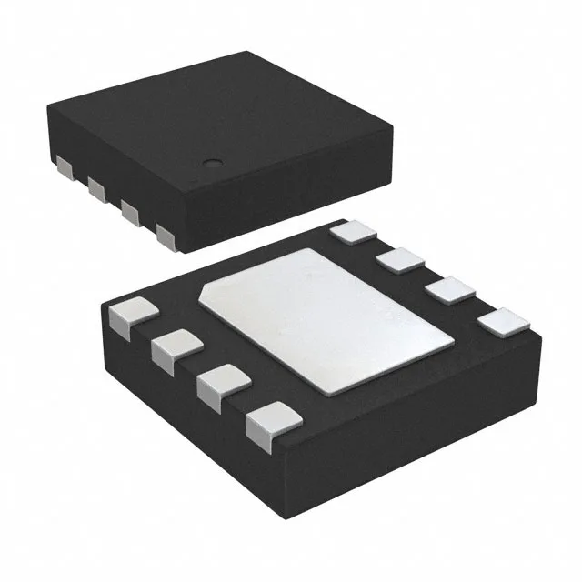
ADP7185ACPZN1.2-R7 -1.2V 500mA Negative LDO, 8-LFCSP

MPNADP7185ACPZN1.2-R7
End of Life

Analog Devices ADP7185ACPZN1.2-R7, Negative Linear Regulator, Fixed -1.2V Output, 500mA, 8-UFDFN Exposed Pad CSP, 80dB PSRR, Active.

$5.49Ref. price · indicative, final on quote
Packaging8-UFDFN Exposed Pad, CSP
StockContact for availability
Lead timeIn Stock wk
MOQ1 pcs
  • 100% new & originalTraceable channels only — no refurbs, no pulls, no remarked parts.
  • Date & lot codes on quoteStated per line before you commit; label photos on request.
  • MSL-compliant ESD packingMoisture-sealed bags with indicator cards; reels photo-verified.
  • PayPal buyer protectionPay by T/T, PayPal or Payoneer — card payments covered end to end.

Specifications

ADP7185ACPZN1.2-R7 Technical Specifications
ParameterValue
Output typeFixed
Mounting typeSurface Mount
Voltage - input-5.5V
Voltage dropout0.36V @ 500mA
Voltage - output (Min (Fixed))-1.2V
Current - output500mA
Current - supply7 mA
Current - quiescent900 µA
Operating temperature-40°C ~ 125°C (TJ)
PSRR80dB ~ 40dB (1kHz ~ 1MHz)
PackageTape & Reel (TR); Cut Tape (CT)
Case8-UFDFN Exposed Pad, CSP
Control featuresEnable, Power On Reset
Protection featuresOver Current
Number of regulators1
Output configurationNegative

Product details

Negative rail regulator for bipolar analog front-ends

The ADP7185ACPZN1.2-R7 is a negative-output low-dropout linear regulator from Analog Devices, delivering a fixed -1.2 V at up to 500 mA. In a dual-supply signal chain — op-amp rails, ADC reference drivers, or sensor bias — this part generates the negative rail from a -5.5 V max input without a switching inverter and its associated ripple. Its power-supply rejection ratio of 80 dB at 1 kHz, rolling off to 40 dB at 1 MHz, means high-frequency noise from the upstream rail is attenuated by a factor of 10,000 at low frequencies, preserving the noise floor of precision analog stages.

Dropout voltage and thermal budget

Maximum dropout is 360 mV at the full 500 mA load. That sets the minimum input-to-output differential: a -1.56 V input rail is the floor to maintain regulation at full current. Below that headroom the output falls out of regulation, so the upstream buck or LDO feeding this part must hold at least -1.56 V under load. Junction temperature range spans -40°C to 125°C, covering automotive under-hood and industrial motor-drive ambient conditions. The 2x2 mm 8-LFCSP exposed pad (UFDFN) package relies on the PCB copper pour under the pad for thermal dissipation — a 1-square-inch pour on a 2-layer board keeps the junction rise below 50°C at 500 mA with 1.5 V dropout.

Control and protection for sequenced rails

Over-current protection limits the output during a fault — the regulator folds back rather than latching off, so a transient short clears without a power cycle. Quiescent current is 900 µA typical, rising to 7 mA maximum under heavy load. In a battery-powered device where the negative rail is always on, that Iq draws about 22 mW from a -2.5 V input — a consideration for standby budgets.

Frequently asked questions

What is the PSRR of ADP7185ACPZN1.2-R7?

The PSRR is 80 dB at 1 kHz, dropping to 40 dB at 1 MHz. This means noise on the input rail is attenuated by a factor of 10,000 at low frequencies and by a factor of 100 at 1 MHz, making it suitable for powering sensitive analog circuits like ADC references or op-amp rails.

What package does ADP7185ACPZN1.2-R7 come in?

It is supplied in an 8-UFDFN Exposed Pad, CSP package (also designated 8-LFCSP, 2x2 mm). Available in Tape & Reel (TR) or Cut Tape (CT) options.

What compliance documentation does Analog Devices provide for ADP7185ACPZN1.2-R7?

The part is ROHS3 compliant. Analog Devices provides a datasheet, RoHS certificate of compliance, and material declaration. No UL or IEC certification is listed in the spec record.